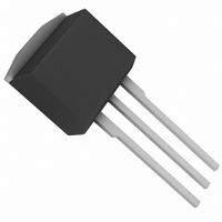
BUK9E06-55A,127 NXP Semiconductors, BUK9E06-55A,127 Datasheet - Page 5

BUK9E06-55A,127
Manufacturer Part Number
BUK9E06-55A,127
Description
MOSFET N-CH TRENCH 55V I2PAK
Manufacturer
NXP Semiconductors
Series
TrenchMOS™r
Specifications of BUK9E06-55A,127
Package / Case
I²Pak, TO-220AB (3 straight leads + tab)
Fet Type
MOSFET N-Channel, Metal Oxide
Fet Feature
Logic Level Gate
Rds On (max) @ Id, Vgs
5.8 mOhm @ 25A, 10V
Drain To Source Voltage (vdss)
55V
Current - Continuous Drain (id) @ 25° C
75A
Vgs(th) (max) @ Id
2V @ 1mA
Input Capacitance (ciss) @ Vds
8600pF @ 25V
Power - Max
300W
Mounting Type
Through Hole
Minimum Operating Temperature
- 55 C
Configuration
Single
Transistor Polarity
N-Channel
Resistance Drain-source Rds (on)
13.2 mOhms
Drain-source Breakdown Voltage
55 V
Gate-source Breakdown Voltage
15 V
Continuous Drain Current
154 A
Power Dissipation
300 W
Maximum Operating Temperature
+ 175 C
Mounting Style
Through Hole
Lead Free Status / RoHS Status
Lead free / RoHS Compliant
Gate Charge (qg) @ Vgs
-
Lead Free Status / Rohs Status
Lead free / RoHS Compliant
Other names
934056832127
8. Characteristics
Table 5:
T
Philips Semiconductors
9397 750 08416
Product data
Symbol
Static characteristics
V
V
I
I
R
Dynamic characteristics
C
C
C
t
t
t
t
L
L
DSS
GSS
d(on)
r
d(off)
f
j
d
s
(BR)DSS
GS(th)
DSon
iss
oss
rss
= 25 C unless otherwise specified
Characteristics
Parameter
drain-source breakdown
voltage
gate-source threshold voltage I
drain-source leakage current
gate-source leakage current
drain-source on-state
resistance
input capacitance
output capacitance
reverse transfer capacitance
turn-on delay time
rise time
turn-off delay time
fall time
internal drain inductance
internal source inductance
Conditions
I
Figure 9
V
V
V
Figure 7
V
V
V
f = 1 MHz;
V
V
from drain lead 6 mm from
package to centre of die
from contact screw on
mounting base to centre of
die SOT78
from upper edge of drain
mounting base to centre of
die SOT404 / SOT226
from source lead to source
bond pad
D
D
DS
GS
GS
GS
GS
GS
DD
GS
T
T
T
T
T
T
T
T
T
= 0.25 mA; V
= 1 mA; V
j
j
j
j
j
j
j
j
j
= 55 V; V
= 25 C
= 55 C
= 25 C
= 175 C
= 55 C
= 25 C
= 175 C
= 10 V; V
= 5 V; I
= 25 C
= 175 C
= 4.5 V; I
= 10 V; I
= 0 V; V
= 30 V; R
= 5 V; R
Rev. 03 — 23 July 2001
and
BUK9506-55A; BUK9606-55A;
Figure 12
D
DS
DS
G
D
8
= 25 A;
D
GS
L
= 10
= 25 A
DS
= V
= 25 A
GS
= 25 V;
= 1.2 ;
= 0 V
= 0 V
= 0 V
GS
;
Min
55
50
1
0.5
BUK9E06-55A
Typ
1.5
0.05
2
5.3
4.8
6500
1000
650
45
180
420
235
4.5
3.5
2.5
7.5
© Philips Electronics N.V. 2001. All rights reserved.
Max
2
2.3
10
500
100
6.3
13.2
6.7
5.8
8600
1200
850
Unit
V
V
V
V
V
nA
m
m
m
m
pF
pF
pF
ns
ns
ns
ns
nH
nH
nH
nH
5 of 16
A
A


