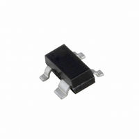
BF909,215 NXP Semiconductors, BF909,215 Datasheet - Page 2

BF909,215
Manufacturer Part Number
BF909,215
Description
MOSFET N-CH 7V 40MA SOT143B
Manufacturer
NXP Semiconductors
Datasheet
1.BF909R235.pdf
(12 pages)
Specifications of BF909,215
Package / Case
SOT-143, SOT-143B, TO-253AA
Current Rating
40mA
Frequency
800MHz
Transistor Type
N-Channel Dual Gate
Noise Figure
2dB
Current - Test
15mA
Voltage - Test
5V
Configuration
Dual
Continuous Drain Current
20 mA
Drain-source Breakdown Voltage
15 V
Gate-source Breakdown Voltage
15 V
Maximum Operating Temperature
+ 150 C
Minimum Operating Temperature
- 65 C
Mounting Style
SMD/SMT
Power Dissipation
200 mW
Transistor Polarity
Dual N-Channel
Lead Free Status / RoHS Status
Lead free / RoHS Compliant
Power - Output
-
Gain
-
Lead Free Status / Rohs Status
Lead free / RoHS Compliant
Other names
934028850215::BF909 T/R::BF909 T/R
NXP Semiconductors
FEATURES
APPLICATIONS
DESCRIPTION
Enhancement type field-effect transistor in a plastic
microminiature SOT143 or SOT143R package. The
QUICK REFERENCE DATA
handbook, halfpage
V
I
P
T
C
C
F
D
y
j
Specially designed for use at 5 V supply voltage
High forward transfer admittance
Short channel transistor with high forward transfer
admittance to input capacitance ratio
Low noise gain controlled amplifier up to 1 GHz
Superior cross-modulation performance during AGC.
VHF and UHF applications with 3 to 7 V supply voltage
such as television tuners and professional
communications equipment.
DS
tot
ig1-s
rs
N-channel dual gate MOS-FETs
BF909 marking code: %M3.
SYMBOL
fs
Top view
Fig.1 Simplified outline (SOT143) and symbol.
4
1
drain-source voltage
drain current
total power dissipation
operating junction temperature
forward transfer admittance
input capacitance at gate 1
reverse transfer capacitance
noise figure
3
2
MAM124
PARAMETER
g
g
2
1
d
Rev. 02 - 19 November 2007
s,b
f = 1 MHz
f = 800 MHz
transistor consists of an amplifier MOS-FET with source
and substrate interconnected and an internal bias circuit to
ensure good cross-modulation performance during AGC.
PINNING
handbook, halfpage
CONDITIONS
The device is supplied in an antistatic package. The
gate-source input must be protected against static
discharge during transport or handling.
Top view
BF909R marking code: %M4.
PIN
Fig.2 Simplified outline (SOT143R) and symbol.
1
2
3
4
3
2
SYMBOL
1
s, b
g
g
d
4
2
1
36
MAM125 - 1
MIN.
CAUTION
source
drain
gate 2
gate 1
43
3.6
35
2
BF909; BF909R
TYP.
DESCRIPTION
g
g
Product specification
2
1
7
40
200
150
50
4.3
50
2.8
MAX.
d
2 of 12
V
mA
mW
mS
pF
fF
dB
C
UNIT
s,b


