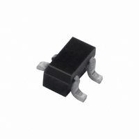
BFR520T,115 NXP Semiconductors, BFR520T,115 Datasheet - Page 2

BFR520T,115
Manufacturer Part Number
BFR520T,115
Description
TRANS NPN 15V 9GHZ SOT-416
Manufacturer
NXP Semiconductors
Datasheet
1.BFR520T115.pdf
(13 pages)
Specifications of BFR520T,115
Package / Case
EMT3 (SOT-416, SC-75-3)
Mounting Type
Surface Mount
Power - Max
150mW
Current - Collector (ic) (max)
70mA
Voltage - Collector Emitter Breakdown (max)
15V
Transistor Type
NPN
Frequency - Transition
9GHz
Dc Current Gain (hfe) (min) @ Ic, Vce
60 @ 20mA, 6V
Noise Figure (db Typ @ F)
1.1dB ~ 1.6dB @ 900MHz
Dc Current Gain Hfe Max
60
Mounting Style
SMD/SMT
Configuration
Single
Transistor Polarity
NPN
Maximum Operating Frequency
9000 MHz
Collector- Emitter Voltage Vceo Max
15 V
Emitter- Base Voltage Vebo
2.5 V
Continuous Collector Current
0.07 A
Power Dissipation
150 mW
Maximum Operating Temperature
+ 150 C
Number Of Elements
1
Collector-emitter Voltage
15V
Collector-base Voltage(max)
20V
Emitter-base Voltage (max)
2.5V
Collector Current (dc) (max)
70mA
Dc Current Gain (min)
60
Frequency (max)
9GHz
Operating Temp Range
-65C to 150C
Operating Temperature Classification
Military
Mounting
Surface Mount
Pin Count
3
Package Type
SC-75
Collector-base Voltage
20V
Emitter-base Voltage
2.5V
Lead Free Status / RoHS Status
Lead free / RoHS Compliant
Gain
-
Lead Free Status / Rohs Status
Compliant
Other names
934055892115::BFR520T T/R::BFR520T T/R
NXP Semiconductors
FEATURES
High power gain
Low noise figure
High transition frequency
Gold metallization ensures
SOT416 (SC-75) package.
APPLICATIONS
Wideband applications such as
satellite TV tuners, cellular phones,
cordless phones, pagers etc., with
signal frequencies up to 2 GHz.
QUICK REFERENCE DATA
Note
1. T
LIMITING VALUES
In accordance with the Absolute Maximum System (IEC 60134).
Note
1. T
2000 Apr 03
V
V
I
P
h
f
G
F
V
V
V
I
P
T
T
C
T
C
SYMBOL
SYMBOL
FE
excellent reliability
stg
j
CBO
CES
tot
CBO
CES
EBO
tot
NPN 9 GHz wideband transistor
UM
s
s
is the temperature at the soldering point of the collector tab.
is the temperature at the soldering point of the collector tab.
collector-base voltage
collector-emitter voltage
DC collector current
total power dissipation
DC current gain
transition frequency
maximum unilateral power
gain
noise figure
collector-base voltage
collector-emitter voltage
emitter-base voltage
DC collector current
total power dissipation
storage temperature
junction temperature
PARAMETER
PARAMETER
DESCRIPTION
Silicon NPN transistor encapsulated
in a plastic SOT416 (SC-75) package.
PINNING
PIN
1
2
3
open emitter
R
up to T
I
I
T
I
T
I
T
open emitter
R
open collector
up to T
C
C
C
C
amb
amb
amb
BE
BE
= 20 mA; V
= 20 mA; V
= 20 mA; V
= 5 mA; V
= 0
= 0
base
emitter
collector
= 25 C
= 25 C
= 25 C
s
s
= 75 C; note 1
= 75 C; note 1
DESCRIPTION
CONDITIONS
CONDITIONS
2
CE
CE
CE
CE
= 6 V; f = 900 MHz;
= 6 V; T
= 6 V; f = 1 GHz;
= 6 V; f = 900 MHz;
j
= 25 C
lfpage
Marking code: N2.
60
65
MIN.
MIN.
Top view
Fig.1 SOT416.
1
120
9
15
1.1
TYP.
Product specification
20
15
2.5
70
150
+150
150
MAX.
3
BFR520T
20
15
70
150
250
1.6
MAX.
MBK090
2
V
V
V
mA
mW
C
C
UNIT
V
V
mA
mW
GHz
dB
dB
UNIT


