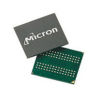
MT48H8M32LFB5-75 IT:H Micron Technology Inc, MT48H8M32LFB5-75 IT:H Datasheet - Page 36

MT48H8M32LFB5-75 IT:H
Manufacturer Part Number
MT48H8M32LFB5-75 IT:H
Description
DRAM Chip Mobile SDRAM 256M-Bit 8Mx32 1.8V 90-Pin VFBGA Tray
Manufacturer
Micron Technology Inc
Type
Mobile SDRAMr
Specifications of MT48H8M32LFB5-75 IT:H
Density
256 Mb
Maximum Clock Rate
133 MHz
Package
90VFBGA
Address Bus Width
14 Bit
Operating Supply Voltage
1.8 V
Maximum Random Access Time
8|6 ns
Operating Temperature
-40 to 85 °C
Format - Memory
RAM
Memory Type
Mobile SDRAM
Memory Size
256M (8Mx32)
Speed
133MHz
Interface
Parallel
Voltage - Supply
1.7 V ~ 1.95 V
Package / Case
90-VFBGA
Organization
8Mx32
Address Bus
14b
Access Time (max)
8/6ns
Operating Supply Voltage (typ)
1.8V
Package Type
VFBGA
Operating Temp Range
-40C to 85C
Operating Supply Voltage (max)
1.95V
Operating Supply Voltage (min)
1.7V
Supply Current
100mA
Pin Count
90
Mounting
Surface Mount
Operating Temperature Classification
Industrial
Lead Free Status / RoHS Status
Lead free / RoHS Compliant
Concurrent Auto Precharge
READ with Auto Precharge
Figure 27:
PDF:09005aef8219eeeb/Source: 09005aef8219eedd
256mb_x16_sdram_y36m_1.fm - Rev G 6/09 EN
Clock Suspend During WRITE Burst
Note:
1. Interrupted by a READ (with or without auto precharge): A READ to bank m will inter-
2. Interrupted by a WRITE (with or without auto precharge): A WRITE to bank m will
An access command (READ or WRITE) to a second bank while an access command with
auto precharge enabled on a first bank is executing is not allowed by SDRAM, unless the
SDRAM supports concurrent auto precharge. Micron SDRAM support concurrent auto
precharge. Four cases where concurrent auto precharge occurs are defined in the “READ
with Auto Precharge” and “WRITE with Auto Precharge” sections.
COMMAND
INTERNAL
ADDRESS
rupt a READ on bank n, CL later. The precharge to bank n will begin when the READ
to bank m is registered (see Figure 29 on page 37).
interrupt a READ on bank n when registered. DQM should be used two clocks prior to
the WRITE command to prevent bus contention. The precharge to bank n will begin
when the WRITE to bank m is registered (see Figure 30 on page 38).
CLOCK
For this example, BL = 4 or greater, and DM is LOW.
CLK
CKE
D
IN
NOP
T0
WRITE
BANK,
COL n
T1
D
n
IN
T2
36
T3
Micron Technology, Inc., reserves the right to change products or specifications without notice.
NOP
n + 1
T4
D
IN
256Mb: x16, x32 Mobile SDRAM
DON’T CARE
T5
n + 2
NOP
D
IN
©2006 Micron Technology, Inc. All rights reserved.
Operations


