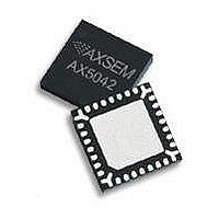
AX5042-QFN28-TU AXSEM, AX5042-QFN28-TU Datasheet - Page 21

AX5042-QFN28-TU
Manufacturer Part Number
AX5042-QFN28-TU
Description
RF Transceiver Narrow-Band-IC
Manufacturer
AXSEM
Datasheet
1.AX5042-QFN28-TU.pdf
(45 pages)
Specifications of AX5042-QFN28-TU
Number Of Receivers
1
Number Of Transmitters
1
Wireless Frequency
433 MHz, 868 MHz, 915 MHz
Interface Type
SPI, UART
Output Power
14.5 dBm
Operating Supply Voltage
2.3 V to 2.8 V
Maximum Operating Temperature
+ 85 C
Maximum Supply Current
54 mA
Minimum Operating Temperature
- 40 C
Modulation
ASK, FSK, PSK
Lead Free Status / RoHS Status
Lead free / RoHS Compliant
5.4.
The
A reset must be applied after power-up. It is safe to perform this power-on reset using a SPI
access, so using the RESET_N pin is strictly optional. If the RESET_N pin is not used it must be
tied to VDD.
5.5.
The DATA input/output pin is used for data transfer from and to
The transfer direction of data is set by programming the
applied to the pin IRQ_TXEN (1=TX, then DATA is an input pin; 0=RX, then DATA is an output
pin).
The DCLK output pin supplies the corresponding data clock which depends on the data-rate
settings programmed to AX5042. In synchronous wire mode a connected micro-controller
must receive or supply data on the DATA pin synchronous to the clock available the DCLK
pin. In asynchronous wire mode, the receive/transmit clock is still available on the DCLK pin,
but its usage is optional.
If frame mode is used for data communication, the pins DCLK and DATA can optionally be
used as general purpose I/O pins.
Version 2.4
1. By SPI accesses: the bit RST in the
2. Via the RESET_N pin: A low pulse is applied at the RESET_N pin. With the rising edge of
AX5042
RESET_N Input
DATA Input/Output and DCLK Output
RESET_N the device goes into its operational state.
can be reset in two ways:
PWRMODE
register is toggled.
PWRMODE
AX5042
register or by the level
in wire mode.
Circuit Description
Datasheet AX5042
21


