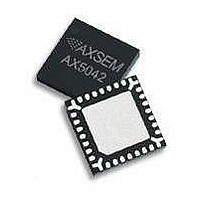
AX5042-QFN28-TU AXSEM, AX5042-QFN28-TU Datasheet - Page 23

AX5042-QFN28-TU
Manufacturer Part Number
AX5042-QFN28-TU
Description
RF Transceiver Narrow-Band-IC
Manufacturer
AXSEM
Datasheet
1.AX5042-QFN28-TU.pdf
(45 pages)
Specifications of AX5042-QFN28-TU
Number Of Receivers
1
Number Of Transmitters
1
Wireless Frequency
433 MHz, 868 MHz, 915 MHz
Interface Type
SPI, UART
Output Power
14.5 dBm
Operating Supply Voltage
2.3 V to 2.8 V
Maximum Operating Temperature
+ 85 C
Maximum Supply Current
54 mA
Minimum Operating Temperature
- 40 C
Modulation
ASK, FSK, PSK
Lead Free Status / RoHS Status
Lead free / RoHS Compliant
Loop Filter and Charge Pump
The
synthesizer loop band width. The loop filter has three configurations that can be
programmed via the register bits FLT[1:0] in register PLLLOOP, the charge pump current can
be programmed using register bits PLLCPI[2:0] also in register PLLLOOP. Synthesizer
bandwidths are typically 50 - 500 kHz depending on the
section 4.3: AC Characteristics.
Registers
Register
PLLLOOP
FREQ
IFFREQHI, IFFREQLO
PLLRANGING
5.7.
The
external RX/TX switch is not required.
LNA
The LNA amplifies the differential RF signal from the antenna and buffers it to drive the I/Q
mixer. An external matching network is used to adapt the antenna impedance to the IC
impedance. A DC feed to the supply voltage VDD must be provided at the antenna pins. For
recommendations see section 7: Application Information.
I/Q mixer
The RF signal from the LNA is mixed down to an IF of typically 1 MHz. I- and Q-IF signals are
buffered for the analog IF filter.
PA
In TX mode the PA drives the signal generated by the frequency generation subsystem out to
the differential antenna terminals. The output power of the PA is programmed via bits
TXRNG[3:0] in the register TXPWR. Output power as well as harmonic content will depend on
the external impedance seen by the PA, recommendations are given in the section 7:
Application Information.
Version 2.4
AX5042
AX5042
RF Input and Output Stage (ANTP/ANTN)
Bits
FLT[1:0]
PLLCPI[2:0]
BANDSEL
internal loop filter configuration together with the charge pump current sets the
uses fully differential antenna pins. RX/TX switching is handled internally, an
Purpose
Synthesizer loop filter bandwidth, recommended usage is to increase the bandwidth
for faster settling time, bandwidth increases of factor 2 and 5 are possible.
Synthesizer charge pump current, recommended usage is to decrease the bandwidth
(and improve the phase-noise) for low data-rate transmissions.
Switches between 868 MHz/915 MHz and 433 MHz bands
Programming of the carrier frequency
Programming of the IF frequency
Initiate VCO auto-ranging and check results
PLLLOOP
settings, for details see
Circuit Description
Datasheet AX5042
23


