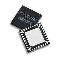
AX5042-QFN28-TU AXSEM, AX5042-QFN28-TU Datasheet - Page 8

AX5042-QFN28-TU
Manufacturer Part Number
AX5042-QFN28-TU
Description
RF Transceiver Narrow-Band-IC
Manufacturer
AXSEM
Datasheet
1.AX5042-QFN28-TU.pdf
(45 pages)
Specifications of AX5042-QFN28-TU
Number Of Receivers
1
Number Of Transmitters
1
Wireless Frequency
433 MHz, 868 MHz, 915 MHz
Interface Type
SPI, UART
Output Power
14.5 dBm
Operating Supply Voltage
2.3 V to 2.8 V
Maximum Operating Temperature
+ 85 C
Maximum Supply Current
54 mA
Minimum Operating Temperature
- 40 C
Modulation
ASK, FSK, PSK
Lead Free Status / RoHS Status
Lead free / RoHS Compliant
8
Pin Function Descriptions
3. Pin Function Descriptions
Symbol
NC
VDD
GND
ANTP
ANTN
GND
VDD
NC
LPFILT
NC
GND
RESET_N
SYSCLK
SEL
CLK
MISO
MOSI
DATA
IRQ_TXEN
VDD
DCLK
GND
PWRUP
NC
NC
VDD
CLK16P
CLK16N
A =
I
O =
All digital inputs are Schmitt trigger inputs, digital input and output levels are LVCMOS/LVTTL compatible and 3.3V/5V
tolerant
The centre pad of the QFN28 package should be connected to GND.
Version 2.4
=
analog signal
digital input signal
digital output signal
.
Pin(s)
10
11
12
13
14
15
16
17
18
19
20
21
22
23
24
25
26
27
28
1
2
3
4
5
6
7
8
9
Type
I/O
I/O
I/O
I/O
I/O
G
O
N
P
A
A
P
P
N
A
N
P
P
P
N
N
P
A
A
I
I
I
I
Description
Power supply
Ground
Antenna input/output
Antenna input/output
Ground
Power supply
Not to be connected
Pin for optional external synthesizer loop filter; leave unconnected if not used
It is recommended to use the internal loop filter
Not to be connected
Ground
Optional reset input. If not used this pin must be connected to VDD.
Default functionality: Crystal oscillator (or divided) clock output
Can be programmed to be used as a general purpose I/O pin
Serial peripheral interface select
Serial peripheral interface clock
Serial peripheral interface data output
Serial peripheral interface data input
In wire mode: Data input/output
Can be programmed to be used as a general purpose I/O pin
In frame mode: Interrupt request output
In wire mode: Transmit enable input
Can be programmed to be used as a general purpose I/O pin
Power supply
In wire mode: Clock output
Can be programmed to be used as a general purpose I/O pin
Ground
Power-up/-down input; activates/deactivates analog blocks
Can be programmed to be used as a general purpose I/O pin
If the power-up/-down functionality is handled in software and no usage as
general purpose I/O pin is planned then this pin should be tied to VDD
Not to be connected
Not to be connected
Power supply
Crystal oscillator input/output
Crystal oscillator input/output
Not to be connected
I/O
N
P
=
=
=
digital input/output signal
not to be connected
power or ground
Datasheet AX5042


