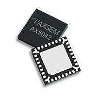
AX5042-QFN28-TU AXSEM, AX5042-QFN28-TU Datasheet - Page 32

AX5042-QFN28-TU
Manufacturer Part Number
AX5042-QFN28-TU
Description
RF Transceiver Narrow-Band-IC
Manufacturer
AXSEM
Datasheet
1.AX5042-QFN28-TU.pdf
(45 pages)
Specifications of AX5042-QFN28-TU
Number Of Receivers
1
Number Of Transmitters
1
Wireless Frequency
433 MHz, 868 MHz, 915 MHz
Interface Type
SPI, UART
Output Power
14.5 dBm
Operating Supply Voltage
2.3 V to 2.8 V
Maximum Operating Temperature
+ 85 C
Maximum Supply Current
54 mA
Minimum Operating Temperature
- 40 C
Modulation
ASK, FSK, PSK
Lead Free Status / RoHS Status
Lead free / RoHS Compliant
32
Circuit Description
5.17. Wire Mode Interface
In wire mode the transmitted or received data are transferred from and to the
the pins DATA and DCLK. DATA is an input when transmitting and an output when receiving.
The direction can be chosen by programming the
using the IRQ_TXEN pin.
Wire mode offers two variants: synchronous or asynchronous.
In synchronous wire mode the, the
applied to DATA synchronously to DCLK, and receive data must be sampled synchronously
to DCLK. Timing is given in Figure 4. Setting the bit DCLKI in register
signal.
In asynchronous wire mode, a low voltage RS232 type UART can be connected to DATA.
DCLK is optional in this mode. The UART must be programmed to send two stop bits, but must
be able to accept only one stop bit. Both the UART data rate and the
receive bit rate must match. The
transmission clock, by inserting or deleting a stop bit.
Registers for setting up the
Wire Mode Timing
Version 2.4
DCLK (DCLKI=0)
DCLK (DCLKI=1)
DATA (RX)
DATA (TX)
AX5042
Tdck
Figure 4 Wire mode interface timing
are programmed via the serial peripheral interface (SPI).
Tdch Tdcl
AX5042
AX5042
synchronizes the RS232 signal to its internal
always drives DCLK. Transmit data must be
Tds
PWRMODE
Tdh
Tdco
register (recommended), or by
PINCFG2
AX5042
inverts the DCLK
Datasheet AX5042
AX5042
transmit and
using


