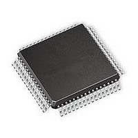
PIC16F1527-E/MR Microchip Technology, PIC16F1527-E/MR Datasheet - Page 145

PIC16F1527-E/MR
Manufacturer Part Number
PIC16F1527-E/MR
Description
64-pin, 28KB Flash, 1536B RAM, 10-bit ADC, 10xCCP, 2xSPI, 2xMI2C, 2xEUSART, 2.3V
Manufacturer
Microchip Technology
Series
PIC® XLP™ 16Fr
Datasheet
1.PIC16F1526-EMR.pdf
(354 pages)
Specifications of PIC16F1527-E/MR
Core Processor
PIC
Core Size
8-Bit
Speed
20MHz
Connectivity
I²C, LIN, SPI, UART/USART
Peripherals
Brown-out Detect/Reset, POR, PWM, WDT
Number Of I /o
54
Program Memory Size
28KB (16K x 14)
Program Memory Type
FLASH
Eeprom Size
-
Ram Size
1.5K x 8
Voltage - Supply (vcc/vdd)
2.3 V ~ 5.5 V
Data Converters
A/D 30x10b
Oscillator Type
Internal
Operating Temperature
-40°C ~ 125°C
Package / Case
64-VFQFN Exposed Pad
Core
PIC
Processor Series
PIC16F
Data Bus Width
8 bit
Maximum Clock Frequency
20 MHz
Data Ram Size
1536 B
Number Of Programmable I/os
54
Operating Supply Voltage
2.3 V to 5.5 V
Mounting Style
SMD/SMT
Interface Type
SPI, I2C
Lead Free Status / Rohs Status
Lead free / RoHS Compliant
- Current page: 145 of 354
- Download datasheet (3Mb)
14.0
The Fixed Voltage Reference, or FVR, is a stable
voltage reference, independent of V
2.048V or 4.096V selectable output levels. The output
of the FVR can be configured to supply a reference
voltage to the following:
• ADC input channel
• ADC positive reference
The FVR can be enabled by setting the FVREN bit of
the FVRCON register.
FIGURE 14-1:
TABLE 14-1:
2011 Microchip Technology Inc.
HFINTOSC
BOR
LDO
Peripheral
FIXED VOLTAGE REFERENCE
(FVR)
FOSC<2:0> = 100 and
IRCF<3:0> = 000x
BOREN<1:0> = 11
BOREN<1:0> = 10 and BORFS = 1
BOREN<1:0> = 01 and BORFS = 1
All PIC16F1526/27 devices, when
VREGPM = 1 and not in Sleep
Any peripheral requiring
PERIPHERALS REQUIRING THE FIXED VOLTAGE REFERENCE (FVR)
the Fixed Reference
FVREN
(See
VOLTAGE REFERENCE BLOCK DIAGRAM
Table
ADFVR<1:0>
Conditions
14-1)
DD
, with 1.024V,
2
+
-
Preliminary
1.024V Fixed
Reference
INTOSC is active and device is not in Sleep.
BOR always enabled.
BOR disabled in Sleep mode, BOR Fast Start enabled.
BOR under software control, BOR Fast Start enabled.
The device runs off of the low-power regulator when in Sleep
mode.
x1
x2
x4
14.1
The output of the FVR supplied to the ADC module is
routed through two independent programmable gain
amplifiers. Each amplifier can be configured to amplify
the reference voltage by 1x, 2x or 4x, to produce the
three possible voltage levels.
The ADFVR<1:0> bits of the FVRCON register are
used to enable and configure the gain amplifier settings
for the reference supplied to the ADC module. Refer-
ence
(ADC) Module”
14.2
When the Fixed Voltage Reference module is enabled, it
requires time for the reference and amplifier circuits to
stabilize. Once the circuits stabilize and are ready for use,
the FVRRDY bit of the FVRCON register will be set. See
Section 25.0 “Electrical Specifications”
minimum delay requirement.
FVRRDY
Section 16.0 “Analog-to-Digital Converter
PIC16(L)F1526/27
Independent Gain Amplifiers
FVR Stabilization Period
for additional information.
Description
(To ADC Module)
FVR BUFFER1
DS41458B-page 145
for the
Related parts for PIC16F1527-E/MR
Image
Part Number
Description
Manufacturer
Datasheet
Request
R

Part Number:
Description:
IC, 8BIT MCU, PIC16F, 32MHZ, SOIC-18
Manufacturer:
Microchip Technology
Datasheet:

Part Number:
Description:
IC, 8BIT MCU, PIC16F, 32MHZ, SSOP-20
Manufacturer:
Microchip Technology
Datasheet:

Part Number:
Description:
IC, 8BIT MCU, PIC16F, 32MHZ, DIP-18
Manufacturer:
Microchip Technology
Datasheet:

Part Number:
Description:
IC, 8BIT MCU, PIC16F, 32MHZ, QFN-28
Manufacturer:
Microchip Technology
Datasheet:

Part Number:
Description:
IC, 8BIT MCU, PIC16F, 32MHZ, QFN-28
Manufacturer:
Microchip Technology
Datasheet:

Part Number:
Description:
IC, 8BIT MCU, PIC16F, 32MHZ, QFN-28
Manufacturer:
Microchip Technology
Datasheet:

Part Number:
Description:
IC, 8BIT MCU, PIC16F, 32MHZ, SSOP-20
Manufacturer:
Microchip Technology
Datasheet:

Part Number:
Description:
IC, 8BIT MCU, PIC16F, 20MHZ, DIP-40
Manufacturer:
Microchip Technology
Datasheet:

Part Number:
Description:
IC, 8BIT MCU, PIC16F, 32MHZ, QFN-28
Manufacturer:
Microchip Technology
Datasheet:

Part Number:
Description:
IC, 8BIT MCU, PIC16F, 20MHZ, MQFP-44
Manufacturer:
Microchip Technology
Datasheet:

Part Number:
Description:
IC, 8BIT MCU, PIC16F, 20MHZ, QFN-20
Manufacturer:
Microchip Technology
Datasheet:

Part Number:
Description:
IC, 8BIT MCU, PIC16F, 32MHZ, QFN-28
Manufacturer:
Microchip Technology
Datasheet:

Part Number:
Description:
MCU 14KB FLASH 768B RAM 64-TQFP
Manufacturer:
Microchip Technology
Datasheet:

Part Number:
Description:
7 KB Flash, 384 Bytes RAM, 32 MHz Int. Osc, 16 I/0, Enhanced Mid Range Core, Low
Manufacturer:
Microchip Technology

Part Number:
Description:
14KB Flash, 512B RAM, 256B EEPROM, LCD, 1.8-5.5V 40 UQFN 5x5x0.5mm TUBE
Manufacturer:
Microchip Technology
Datasheet:


