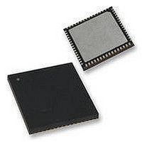
PIC24FJ64GA106-I/MR Microchip Technology, PIC24FJ64GA106-I/MR Datasheet - Page 180

PIC24FJ64GA106-I/MR
Manufacturer Part Number
PIC24FJ64GA106-I/MR
Description
16-bit, 16 MIPS, 64KB Flash, 16Kb RAM, 84 I/O, NanoWatt 64 QFN 9x9x0.9mm TUBE
Manufacturer
Microchip Technology
Series
PIC® 24Fr
Datasheet
1.PIC24FJ128GA106-IPT.pdf
(330 pages)
Specifications of PIC24FJ64GA106-I/MR
Core Processor
PIC
Core Size
16-Bit
Speed
32MHz
Connectivity
I²C, IrDA, LIN, SPI, UART/USART
Peripherals
Brown-out Detect/Reset, LVD, POR, PWM, WDT
Number Of I /o
53
Program Memory Size
64KB (22K x 24)
Program Memory Type
FLASH
Ram Size
16K x 8
Voltage - Supply (vcc/vdd)
2 V ~ 3.6 V
Data Converters
A/D 16x10b
Oscillator Type
Internal
Operating Temperature
-40°C ~ 85°C
Package / Case
64-VFQFN Exposed Pad
Processor Series
PIC24FJ256GA110
Core
PIC
Data Bus Width
16 bit
Data Ram Size
16 KB
Interface Type
UART, I2C, SPI
Maximum Clock Frequency
8 MHz
Number Of Timers
5
Operating Supply Voltage
3.6 V
Maximum Operating Temperature
- 40 C to + 85 C
Mounting Style
SMD/SMT
Lead Free Status / RoHS Status
Lead free / RoHS Compliant
Eeprom Size
-
Lead Free Status / Rohs Status
Details
- Current page: 180 of 330
- Download datasheet (3Mb)
PIC24FJ256GA110 FAMILY
REGISTER 15-2:
DS39905E-page 180
bit 15
bit 7
Legend:
R = Readable bit
-n = Value at POR
bit 15-13
bit 12
bit 11
bit 10
bit 9
bit 8
bit 7
bit 6
bit 5
Note 1:
SSEN
R/W-0
U-0
—
2:
3:
4:
(4)
If DISSCK = 0, SCKx must be configured to an available RPn pin (or to ASCK1 for SPI1). See
Section 10.4 “Peripheral Pin Select”
If DISSDO = 0, SDOx must be configured to an available RPn pin. See
Select”
The CKE bit is not used in the Framed SPI modes. The user should program this bit to ‘0’ for the Framed
SPI modes (FRMEN = 1).
If SSEN = 1, SSx must be configured to an available RPn pin. See
for more information.
Unimplemented: Read as ‘0’
DISSCK: Disable SCKx pin bit (SPI Master modes only)
1 = Internal SPI clock is disabled; pin functions as I/O
0 = Internal SPI clock is enabled
DISSDO: Disable SDOx pin bit
1 = SDOx pin is not used by module; pin functions as I/O
0 = SDOx pin is controlled by the module
MODE16: Word/Byte Communication Select bit
1 = Communication is word-wide (16 bits)
0 = Communication is byte-wide (8 bits)
SMP: SPIx Data Input Sample Phase bit
Master mode:
1 = Input data sampled at end of data output time
0 = Input data sampled at middle of data output time
Slave mode:
SMP must be cleared when SPIx is used in Slave mode.
CKE: SPIx Clock Edge Select bit
1 = Serial output data changes on transition from active clock state to Idle clock state (see bit 6)
0 = Serial output data changes on transition from Idle clock state to active clock state (see bit 6)
SSEN: Slave Select Enable (Slave mode) bit
1 = SSx pin used for Slave mode
0 = SSx pin not used by module; pin controlled by port function
CKP: Clock Polarity Select bit
1 = Idle state for clock is a high level; active state is a low level
0 = Idle state for clock is a low level; active state is a high level
MSTEN: Master Mode Enable bit
1 = Master mode
0 = Slave mode
R/W-0
CKP
for more information.
U-0
—
SPI
X
CON1: SPIx CONTROL REGISTER 1
W = Writable bit
‘1’ = Bit is set
MSTEN
R/W-0
U-0
—
DISSCK
(2)
SPRE2
R/W-0
R/W-0
(3)
for more information.
(1)
U = Unimplemented bit, read as ‘0’
‘0’ = Bit is cleared
(4)
DISSDO
SPRE1
R/W-0
R/W-0
(2)
(1)
MODE16
SPRE0
R/W-0
R/W-0
Section 10.4 “Peripheral Pin Select”
Section 10.4 “Peripheral Pin
2010 Microchip Technology Inc.
x = Bit is unknown
PPRE1
R/W-0
R/W-0
SMP
PPRE0
CKE
R/W-0
R/W-0
(3)
bit 8
bit 0
Related parts for PIC24FJ64GA106-I/MR
Image
Part Number
Description
Manufacturer
Datasheet
Request
R

Part Number:
Description:
Manufacturer:
Microchip Technology Inc.
Datasheet:

Part Number:
Description:
Manufacturer:
Microchip Technology Inc.
Datasheet:

Part Number:
Description:
Manufacturer:
Microchip Technology Inc.
Datasheet:

Part Number:
Description:
Manufacturer:
Microchip Technology Inc.
Datasheet:

Part Number:
Description:
Manufacturer:
Microchip Technology Inc.
Datasheet:

Part Number:
Description:
Manufacturer:
Microchip Technology Inc.
Datasheet:

Part Number:
Description:
Manufacturer:
Microchip Technology Inc.
Datasheet:

Part Number:
Description:
Manufacturer:
Microchip Technology Inc.
Datasheet:


