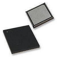
PIC24FJ64GA106-I/MR Microchip Technology, PIC24FJ64GA106-I/MR Datasheet - Page 254

PIC24FJ64GA106-I/MR
Manufacturer Part Number
PIC24FJ64GA106-I/MR
Description
16-bit, 16 MIPS, 64KB Flash, 16Kb RAM, 84 I/O, NanoWatt 64 QFN 9x9x0.9mm TUBE
Manufacturer
Microchip Technology
Series
PIC® 24Fr
Datasheet
1.PIC24FJ128GA106-IPT.pdf
(330 pages)
Specifications of PIC24FJ64GA106-I/MR
Core Processor
PIC
Core Size
16-Bit
Speed
32MHz
Connectivity
I²C, IrDA, LIN, SPI, UART/USART
Peripherals
Brown-out Detect/Reset, LVD, POR, PWM, WDT
Number Of I /o
53
Program Memory Size
64KB (22K x 24)
Program Memory Type
FLASH
Ram Size
16K x 8
Voltage - Supply (vcc/vdd)
2 V ~ 3.6 V
Data Converters
A/D 16x10b
Oscillator Type
Internal
Operating Temperature
-40°C ~ 85°C
Package / Case
64-VFQFN Exposed Pad
Processor Series
PIC24FJ256GA110
Core
PIC
Data Bus Width
16 bit
Data Ram Size
16 KB
Interface Type
UART, I2C, SPI
Maximum Clock Frequency
8 MHz
Number Of Timers
5
Operating Supply Voltage
3.6 V
Maximum Operating Temperature
- 40 C to + 85 C
Mounting Style
SMD/SMT
Lead Free Status / RoHS Status
Lead free / RoHS Compliant
Eeprom Size
-
Lead Free Status / Rohs Status
Details
- Current page: 254 of 330
- Download datasheet (3Mb)
PIC24FJ256GA110 FAMILY
25.4.2
In addition to global General Segment protection, a
separate subrange of the program memory space can
be individually protected against writes and erases.
This area can be used for many purposes where a
separate block of erase and write-protected code is
needed, such as bootloader applications. Unlike
common boot block implementations, the specially pro-
tected segment in the PIC24FJ256GA110 family
devices can be located by the user anywhere in the
program space and configured in a wide range of sizes.
Code segment protection provides an added level of
protection to a designated area of program memory by
disabling the NVM safety interlock whenever a write or
erase address falls within a specified range. It does not
override General Segment protection controlled by the
GCP or GWRP bits. For example, if GCP and GWRP
are enabled, enabling segmented code protection for
the bottom half of program memory does not undo
General Segment protection for the top half.
The size and type of protection for the segmented code
range are configured by the WPFPx, WPEND, WPCFG
and WPDIS bits in Flash Configuration Word 3. Code
segment protection is enabled by programming the
WPDIS bit (= 0). The WPFP bits specify the size of the
segment to be protected by specifying the 512-word
code page that is the start or end of the protected
segment. The specified region is inclusive, therefore,
this page will also be protected.
The WPEND bit determines if the protected segment
uses the top or bottom of the program space as a
boundary. Programming WPEND (= 0) sets the bottom
of program memory (000000h) as the lower boundary
of
TABLE 25-2:
DS39905E-page 254
WPDIS
Segment Configuration Bits
the
1
0
0
0
protected
CODE SEGMENT PROTECTION
WPEND
x
1
0
0
SEGMENT CODE PROTECTION CONFIGURATION OPTIONS
segment.
WPCFG
x
x
1
0
Leaving
No additional protection enabled; all program memory protection is configured
by GCP and GWRP
Addresses from the first address of code page, defined by WPFP<7:0> through
the end of implemented program memory (inclusive), are write/erase protected
including Flash Configuration Words
Address, 000000h through the last address of code page, defined by
WPFP<7:0> (inclusive), is protected
Address, 000000h through the last address of code page, defined by
WPFP<7:0> (inclusive) are write/erase protected and the last page is also
write/erase protected.
WPEND
Write/Erase Protection of Code Segment
segment in the bottom of memory, as well as the Flash
unprogrammed (= 1) protects the specified page
through the last page of implemented program
memory, including the Configuration Word locations.
A separate bit, WPCFG, is used to independently protect
the last page of program space, including the Flash Con-
figuration Words. If WPEND is set to protect the bottom
of program memory, programming WPCFG (= 0) pro-
tects the last page. This may be useful in circumstances
where write protection is needed for both a code
Configuration Words.
The various options for segment code protection are
shown in
25.4.3
The Configuration registers are protected against
inadvertent or unwanted changes, or reads in two
ways. The primary protection method is the same as
that of the RP registers – shadow registers contain a
complimentary value which is constantly compared
with the actual value.
To safeguard against unpredictable events, Configura-
tion bit changes resulting from individual cell level
disruptions (such as ESD events) will cause a parity
error and trigger a device Reset.
The data for the Configuration registers is derived from
the Flash Configuration Words in program memory.
When the GCP bit is set, the source data for device
configuration is also protected as a consequence. Even
if General Segment protection is not enabled, the
device configuration can be protected by using the
appropriate code segment protection setting.
Table
CONFIGURATION REGISTER
PROTECTION
25-2.
2010 Microchip Technology Inc.
Related parts for PIC24FJ64GA106-I/MR
Image
Part Number
Description
Manufacturer
Datasheet
Request
R

Part Number:
Description:
Manufacturer:
Microchip Technology Inc.
Datasheet:

Part Number:
Description:
Manufacturer:
Microchip Technology Inc.
Datasheet:

Part Number:
Description:
Manufacturer:
Microchip Technology Inc.
Datasheet:

Part Number:
Description:
Manufacturer:
Microchip Technology Inc.
Datasheet:

Part Number:
Description:
Manufacturer:
Microchip Technology Inc.
Datasheet:

Part Number:
Description:
Manufacturer:
Microchip Technology Inc.
Datasheet:

Part Number:
Description:
Manufacturer:
Microchip Technology Inc.
Datasheet:

Part Number:
Description:
Manufacturer:
Microchip Technology Inc.
Datasheet:


