SST89E58RD2-40-I-NJE Microchip Technology, SST89E58RD2-40-I-NJE Datasheet - Page 11
SST89E58RD2-40-I-NJE
Manufacturer Part Number
SST89E58RD2-40-I-NJE
Description
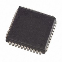
4.5 To 5.5V FlashFlex 8-bit 8051 Microcontroller 44 PLCC TUBE
Manufacturer
Microchip Technology
Series
FlashFlex®r
Specifications of SST89E58RD2-40-I-NJE
Core Processor
8051
Core Size
8-Bit
Speed
40MHz
Connectivity
EBI/EMI, SPI, UART/USART
Peripherals
Brown-out Detect/Reset, POR, WDT
Number Of I /o
36
Program Memory Size
32KB (32K x 8)
Program Memory Type
FLASH
Eeprom Size
8K x 8
Ram Size
1K x 8
Voltage - Supply (vcc/vdd)
4.5 V ~ 5.5 V
Oscillator Type
External
Operating Temperature
-40°C ~ 85°C
Package / Case
44-LCC (J-Lead)
Processor Series
FlashFlex51
Core
C51
Data Bus Width
8 bit
Data Ram Size
1 KB
Interface Type
SPI
Maximum Clock Frequency
40 MHz
Number Of Programmable I/os
5
Number Of Timers
3
Operating Supply Voltage
4.5 V to 5.5 V
Maximum Operating Temperature
+ 85 C
Mounting Style
SMD/SMT
Minimum Operating Temperature
- 40 C
Lead Free Status / RoHS Status
Lead free / RoHS Compliant
Data Converters
-
Lead Free Status / Rohs Status
Details
Available stocks
Company
Part Number
Manufacturer
Quantity
Price
Company:

Part Number:
SST89E58RD2-40-I-NJE
Manufacturer:
Microchip Technology
Quantity:
10 000
Part Number:
SST89E58RD2-40-I-NJE
Manufacturer:
SST
Quantity:
20 000


FlashFlex MCU
SST89E54RD2A/RDA / SST89E58RD2A/RDA
TABLE
©2008 Silicon Storage Technology, Inc.
P4[2] / INT3#
P4[3] / INT2#
ALE/PROG#
1. I = Input; O = Output
2.ALE loading issue: When ALE pin experiences higher loading (>30pf) during the reset, the MCU may accidentally enter into modes
3. For 6 clock mode, ALE is emitted at 1/3 of crystal frequency.
4. Port 4 is not present on the PDIP package.
Symbol
P4[3:0]
PSEN#
XTAL1
XTAL2
P3[2]
P3[3]
P3[4]
P3[5]
P3[6]
P3[7]
P4[0]
P4[1]
RST
EA#
V
V
other than normal working mode. The solution is to add a pull-up resistor of 3-50 KΩ to V
DD
SS
4
2-1: Pin Descriptions (Continued) (2 of 2)
I/O with internal
pull-ups
Type
I/O
I/O
I/O
I/O
I/O
I/O
O
O
O
I
I
I
I
I
I
I
I
I
1
Name and Functions
INT0#: External Interrupt 0 Input
INT1#: External Interrupt 1 Input
T0: External count input to Timer/Counter 0
T1: External count input to Timer/Counter 1
WR#: External Data Memory Write strobe
RD#: External Data Memory Read strobe
Program Store Enable: PSEN# is the Read strobe to External Program Store. When the
device is executing from Internal Program Memory, PSEN# is inactive (V
device is executing code from External Program Memory, PSEN# is activated twice each
machine cycle, except when access to External Data Memory while one PSEN# activation
is skipped in each machine cycle. A forced high-to-low input transition on the PSEN# pin
while the RST input is continually held high for more than 20 machine cycles will cause the
device to enter External Host mode for programming.
Reset: While the oscillator is running, a high logic state on this pin for two machine cycles
will reset the device. After a reset, if the PSEN# pin is driven by a high-to-low input transition
while the RST input pin is held high, the device will enter the External Host mode, otherwise
the device will enter the Normal operation mode.
External Access Enable: EA# must be driven to V
code from the External Program Memory. EA# must be driven to V
execution. However, Security lock level 4 will disable EA#, and program execution is only
possible from internal program memory.
Address Latch Enable: ALE is the output signal for latching the low byte of the address
during an access to external memory. This pin is also the programming pulse input
(PROG#) for flash programming. Normally the ALE
crystal frequency
skipped during each access to external data memory. However, if AO is set to 1, ALE is dis-
abled.
Port 4: Port 4 is an 4-bit bi-directional I/O port with internal pull-ups. The port 4 output buff-
ers can drive LS TTL inputs. Port 4 pins are pulled high by the internal pull-ups when ‘1’s are
written to them and can be used as inputs in this state. As inputs, port 4 pins that are exter-
nally pulled low will source current because of the internal pull-ups.
Bit 0 of port 4
Bit 1 of port 4
Bit 2 of port 4 / INT3# External interrupt 3 input
Bit 3 of port 4 / INT2# External interrupt 2 input
Crystal 1: Input to the inverting oscillator amplifier and input to the internal clock generator
circuits.
Crystal 2: Output from the inverting oscillator amplifier
Power Supply
Ground
3
and can be used for external timing and clocking. One ALE pulse is
11
DD
2
IL
, e.g. for ALE pin.
is emitted at a constant rate of 1/6 the
in order to enable the device to fetch
IH
for internal program
OH
S71339-02-000
). When the
Data Sheet
T2-1.0 1339
02/08
Related parts for SST89E58RD2-40-I-NJE
Image
Part Number
Description
Manufacturer
Datasheet
Request
R

Part Number:
Description:
4.5 To 5.5V FlashFlex 8-bit 8051 Microcontroller 44 TQFP 10x10x1mm TRAY
Manufacturer:
Microchip Technology
Datasheet:

Part Number:
Description:
4.5 To 5.5V FlashFlex 8-bit 8051 Microcontroller 44 PLCC TUBE
Manufacturer:
Microchip Technology
Datasheet:
Part Number:
Description:
4.5 To 5.5V FlashFlex 8-bit 8051 Microcontroller 44 TQFP 10x10x1mm TRAY
Manufacturer:
Microchip Technology
Datasheet:

Part Number:
Description:
Manufacturer:
Microchip Technology Inc.
Datasheet:
Part Number:
Description:
Manufacturer:
Microchip Technology Inc.
Datasheet:
Part Number:
Description:
Manufacturer:
Microchip Technology Inc.
Datasheet:
Part Number:
Description:
Manufacturer:
Microchip Technology Inc.
Datasheet:
Part Number:
Description:
Manufacturer:
Microchip Technology Inc.
Datasheet:
Part Number:
Description:
Manufacturer:
Microchip Technology Inc.
Datasheet:
Part Number:
Description:
Manufacturer:
Microchip Technology Inc.
Datasheet: