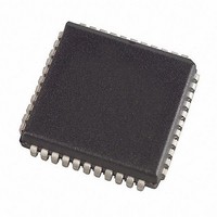
SST89E58RD2-40-I-NJE Microchip Technology, SST89E58RD2-40-I-NJE Datasheet - Page 65

SST89E58RD2-40-I-NJE
Manufacturer Part Number
SST89E58RD2-40-I-NJE
Description
4.5 To 5.5V FlashFlex 8-bit 8051 Microcontroller 44 PLCC TUBE
Manufacturer
Microchip Technology
Series
FlashFlex®r
Specifications of SST89E58RD2-40-I-NJE
Core Processor
8051
Core Size
8-Bit
Speed
40MHz
Connectivity
EBI/EMI, SPI, UART/USART
Peripherals
Brown-out Detect/Reset, POR, WDT
Number Of I /o
36
Program Memory Size
32KB (32K x 8)
Program Memory Type
FLASH
Eeprom Size
8K x 8
Ram Size
1K x 8
Voltage - Supply (vcc/vdd)
4.5 V ~ 5.5 V
Oscillator Type
External
Operating Temperature
-40°C ~ 85°C
Package / Case
44-LCC (J-Lead)
Processor Series
FlashFlex51
Core
C51
Data Bus Width
8 bit
Data Ram Size
1 KB
Interface Type
SPI
Maximum Clock Frequency
40 MHz
Number Of Programmable I/os
5
Number Of Timers
3
Operating Supply Voltage
4.5 V to 5.5 V
Maximum Operating Temperature
+ 85 C
Mounting Style
SMD/SMT
Minimum Operating Temperature
- 40 C
Lead Free Status / RoHS Status
Lead free / RoHS Compliant
Data Converters
-
Lead Free Status / Rohs Status
Details
Available stocks
Company
Part Number
Manufacturer
Quantity
Price
Company:
Part Number:
SST89E58RD2-40-I-NJE
Manufacturer:
Microchip Technology
Quantity:
10 000
Part Number:
SST89E58RD2-40-I-NJE
Manufacturer:
SST
Quantity:
20 000
FlashFlex MCU
SST89E54RD2A/RDA / SST89E58RD2A/RDA
13.0 SYSTEM CLOCK AND CLOCK OPTIONS
13.1 Clock Input Options and Recom-
mended Capacitor Values for Oscillator
Shown in Figure 13-1 are the input and output of an inter-
nal inverting amplifier (XTAL1, XTAL2), which can be con-
figured for use as an on-chip oscillator.
When driving the device from an external clock source,
XTAL2 should be left disconnected and XTAL1 should be
driven.
At start-up, the external oscillator may encounter a higher
capacitive load at XTAL1 due to interaction between the
amplifier and its feedback capacitance. However, the
capacitance will not exceed 15 pF once the external signal
meets the V
Crystal manufacturer, supply voltage, and other factors
may cause circuit performance to differ from one applica-
tion to another. C1 and C2 should be adjusted appropri-
ately for each design. Table 13-1, shows the typical values
for C1 and C2 vs. crystal type for various frequencies
TABLE 13-2: Clock Doubling Features
©2008 Silicon Storage Technology, Inc.
Device
SST89E5xRD2A/RDA
FIGURE 13-1: Oscillator Characteristics
IL
and V
Using the On-Chip Oscillator
IH
C 1
C 2
specifications.
Machine Cycle
Clocks per
12
Standard Mode (x1)
XTAL2
XTAL1
V
Max. External Clock Frequency
SS
(MHz)
40
65
TABLE 13-1:Recommended Values for C1 and
More specific information about on-chip oscillator design
can be found in the FlashFlex Oscillator Circuit Design
Considerations application note.
13.2 Clock Doubling Option
By default, the device runs at 12 clocks per machine cycle
(x1 mode). The device has a clock doubling option to
speed up to 6 clocks per machine cycle. Please refer to
Table 13-2 for detail.
Clock double mode can be enabled either via the external
host mode or the IAP mode. Please refer to Table 4-2 for
the IAP mode enabling commands (When set, the EDC#
bit in SFST register will indicate 6 clock mode.).
The clock double mode is only for doubling the inter-
nal system clock and the internal flash memory, i.e.
EA#=1. To access the external memory and the peripheral
devices, careful consideration must be taken. Also note
that the crystal output (XTAL2) will not be doubled.
Ceramic
Crystal
Machine Cycle
Quartz
Clocks per
Oscillator
External
Signal
C2 by Crystal Type
6
External Clock Drive
Clock Double Mode (x2)
NC
Max. External Clock Frequency
XTAL2
XTAL1
V
SS
(MHz)
C1 = C2
20-30pF
40-50pF
S71339-02-000
20
1339 F32.0
Data Sheet
T13-1.0 1339
T13-2.0 1339
02/08


