SST89E58RD2-40-I-NJE Microchip Technology, SST89E58RD2-40-I-NJE Datasheet - Page 48
SST89E58RD2-40-I-NJE
Manufacturer Part Number
SST89E58RD2-40-I-NJE
Description
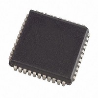
4.5 To 5.5V FlashFlex 8-bit 8051 Microcontroller 44 PLCC TUBE
Manufacturer
Microchip Technology
Series
FlashFlex®r
Specifications of SST89E58RD2-40-I-NJE
Core Processor
8051
Core Size
8-Bit
Speed
40MHz
Connectivity
EBI/EMI, SPI, UART/USART
Peripherals
Brown-out Detect/Reset, POR, WDT
Number Of I /o
36
Program Memory Size
32KB (32K x 8)
Program Memory Type
FLASH
Eeprom Size
8K x 8
Ram Size
1K x 8
Voltage - Supply (vcc/vdd)
4.5 V ~ 5.5 V
Oscillator Type
External
Operating Temperature
-40°C ~ 85°C
Package / Case
44-LCC (J-Lead)
Processor Series
FlashFlex51
Core
C51
Data Bus Width
8 bit
Data Ram Size
1 KB
Interface Type
SPI
Maximum Clock Frequency
40 MHz
Number Of Programmable I/os
5
Number Of Timers
3
Operating Supply Voltage
4.5 V to 5.5 V
Maximum Operating Temperature
+ 85 C
Mounting Style
SMD/SMT
Minimum Operating Temperature
- 40 C
Lead Free Status / RoHS Status
Lead free / RoHS Compliant
Data Converters
-
Lead Free Status / Rohs Status
Details
Available stocks
Company
Part Number
Manufacturer
Quantity
Price
Company:

Part Number:
SST89E58RD2-40-I-NJE
Manufacturer:
Microchip Technology
Quantity:
10 000
Part Number:
SST89E58RD2-40-I-NJE
Manufacturer:
SST
Quantity:
20 000


Data Sheet
8.0 PROGRAMMABLE COUNTER ARRAY
The Programmable Counter Array (PCA) present on the
SST89E/V5xRD2A/RDA is a special 16-bit timer that has
five 16-bit capture/compare modules. Each of the modules
can be programmed to operate in one of four modes: rising
and/or falling edge capture, software timer, high-speed out-
put, or pulse width modulator. The 5th module can be pro-
grammed as a Watchdog Timer in addition to the other four
modes. Each module has a pin associated with it in port 1.
Module 0 is connected to P1.3 (CEX0), module 1 to P1[4]
(CEX1), module 2 to P1[5] (CEX2), module 3 to P1[6]
(CEX3), and module 4 to P1[7] (CEX4). PCA configuration
is shown in Figure 8-1.
8.1 PCA Overview
PCA provides more timing capabilities with less CPU inter-
vention than the standard timer/counter. Its advantages
include reduced software overhead and improved accuracy.
The PCA consists of a dedicated timer/counter which
serves as the time base for an array of five compare/cap-
ture modules. Figure 8-1 shows a block diagram of the
TABLE
©2008 Silicon Storage Technology, Inc.
FIGURE
CPS1
0
0
1
1
8-1: PCA Timer/Counter Source
CPS0
8-1: PCA Timer/Counter and Compare/Capture Modules
0
1
0
1
PCA Timer/Counter
16 Bits
(maximum rate = f
External clock at ECI pin
Timer 0 overflow
12 Clock Mode
f
OSC
f
OSC
/12
/4
OSC
SST89E54RD2A/RDA / SST89E58RD2A/RDA
/8)
48
16 Bits Each
Module 0
Module 1
Module 2
Module 3
Module 4
PCA. External events associated with modules are shared
with corresponding Port 1 pins. Modules not using the port
pins can still be used for standard I/O.
Each of the five modules can be programmed in any of the
following modes:
•
•
•
•
•
8.2 PCA Timer/Counter
The PCA timer is a free-running 16-bit timer consisting of
registers CH and CL (the high and low bytes of the count
values). The PCA timer is common time base for all five
modules and can be programmed to run at: 1/6 the oscilla-
tor frequency, 1/2 the oscillator frequency, Timer 0 overflow,
or the input on the ECI pin (P1.2). The timer/counter source
is determined from the CPS1 and CPS0 bits in the CMOD
SFR as follows (see “PCA Timer/Counter Mode Register
(CMOD)” on page 29):
Rising and/or falling edge capture
Software timer
High speed output
Watchdog Timer (Module 4 only)
Pulse Width Modulator (PWM)
(maximum rate = f
External clock at ECI pin
P1.3/CEX0
P1.4/CEX1
P1.5/CEX2
P1.6/CEX3
P1.7/CEX4
1339 F23.0
Timer 0 overflow
6 Clock Mode
f
f
OSC
OSC
/6
/2
FlashFlex MCU
OSC
S71339-02-000
/4)
T8-1.0 1339
02/08
Related parts for SST89E58RD2-40-I-NJE
Image
Part Number
Description
Manufacturer
Datasheet
Request
R

Part Number:
Description:
4.5 To 5.5V FlashFlex 8-bit 8051 Microcontroller 44 TQFP 10x10x1mm TRAY
Manufacturer:
Microchip Technology
Datasheet:

Part Number:
Description:
4.5 To 5.5V FlashFlex 8-bit 8051 Microcontroller 44 PLCC TUBE
Manufacturer:
Microchip Technology
Datasheet:
Part Number:
Description:
4.5 To 5.5V FlashFlex 8-bit 8051 Microcontroller 44 TQFP 10x10x1mm TRAY
Manufacturer:
Microchip Technology
Datasheet:

Part Number:
Description:
Manufacturer:
Microchip Technology Inc.
Datasheet:
Part Number:
Description:
Manufacturer:
Microchip Technology Inc.
Datasheet:
Part Number:
Description:
Manufacturer:
Microchip Technology Inc.
Datasheet:
Part Number:
Description:
Manufacturer:
Microchip Technology Inc.
Datasheet:
Part Number:
Description:
Manufacturer:
Microchip Technology Inc.
Datasheet:
Part Number:
Description:
Manufacturer:
Microchip Technology Inc.
Datasheet:
Part Number:
Description:
Manufacturer:
Microchip Technology Inc.
Datasheet: