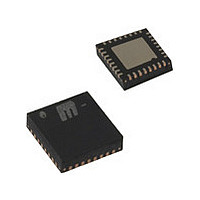
KSZ8851SNLI Micrel Inc, KSZ8851SNLI Datasheet - Page 12

KSZ8851SNLI
Manufacturer Part Number
KSZ8851SNLI
Description
Manufacturer
Micrel Inc
Datasheet
1.KSZ8851SNLI.pdf
(80 pages)
Specifications of KSZ8851SNLI
Operating Supply Voltage (typ)
3.3V
Operating Temperature Classification
Industrial
Mounting
Surface Mount
Pin Count
32
Lead Free Status / RoHS Status
Supplier Unconfirmed
Available stocks
Company
Part Number
Manufacturer
Quantity
Price
Part Number:
KSZ8851SNLI
Manufacturer:
MICROCHIP/微芯
Quantity:
20 000
Company:
Part Number:
KSZ8851SNLI TR
Manufacturer:
Kendin
Quantity:
700
Company:
Part Number:
KSZ8851SNLI TR
Manufacturer:
Micrel
Quantity:
250
Company:
Part Number:
KSZ8851SNLI-TR
Manufacturer:
MXIC
Quantity:
15 000
Company:
Part Number:
KSZ8851SNLITR
Manufacturer:
MICREL
Quantity:
3 500
Part Number:
KSZ8851SNLITR
Manufacturer:
MICREL/麦瑞
Quantity:
20 000
Legend:
P = Power supply
I/O = Bi-directional I = Input O = Output.
Ipd = Input with internal pull-down (58K +/-30%).
Ipu = Input with internal pull-up (58K +/-30%).
Opd = Output with internal pull-down (58K +/-30%).
Opu = Output with internal pull-up (58K +/-30%).
Ipu/O = Input with internal pull-up (58K +/-30%) during power-up/reset; output pin otherwise.
Ipd/O = Input with internal pull-down (58K +/-30%) during power-up/reset; output pin otherwise.
Strapping Options
Note: Ipd/O = Input with internal pull-down (58K +/-30%) during power-up/reset; output pin otherwise.
August 2009
Micrel, Inc.
Pin Number
Pin Number
Pin strap-ins are latched during power-up or reset.
20
21
22
23
24
25
26
27
28
29
30
31
32
6
Gnd = Ground
VDD_D1.8
Pin Name
Pin Name
VDD_IO
VDD_IO
EED_IO
DGND
DGND
DGND
SCLK
LED1
CSN
SO
X1
X2
SI
Ipd/O
Type
Type
Gnd
Gnd
Gnd
Opu
Ipu
Ipd
O
P
P
O
P
I
I
Pin Function
Hardware reset pin (active Low). This reset input must be held low for a minimum of 10ms
after stable supply voltage 3.3V.
25MHz crystal or oscillator clock connection.
Pins (X1, X2) connect to a crystal. If an oscillator is used, X1 connects to a 3.3V tolerant
oscillator and X2 is a no connect.
Note: Clock requirement is +/- 50ppm for either crystal or oscillator.
Digital IO ground
1.8V digital power supply from VDD_CO1.8 (pin 5) with appropriate filtering. If VDD_IO is
1.8V, this pin must be supplied power from the same source as pins 25 and 30 (VDD_IO)
with appropriate filtering.
Digital IO ground
3.3V, 2.5V or 1.8V digital V
SPI slave mode: Chip Select Not
Active low input pin for SPI interface.
SPI slave mode: Serial data out for SPI interface. This SO is tri-stated output when CSN
is negated and this pin must have external 4.7K pull-up to keep the SO line high while the
driver is tri-stated.
SPI slave mode: Serial clock input for SPI interface. This clock speed can run up to
40MHz.
Digital IO ground
3.3V, 2.5V or 1.8V digital V
SPI slave mode: Serial data in for SPI interface.
Programmable LED1 output to indicate PHY activity/status (see LED0 description at pin1)
Pin Function
EEPROM select:
Pull-up = EEPROM present
Floating (NC) or Pull-down = EEPROM not present (default)
During power-up / reset, this pin value is latched into register CCR, bit 9
12
DD
DD
input power supply for IO with well decoupling capacitors.
input power supply for IO with well decoupling capacitors.
KSZ8851SNL/SNLI
M9999-083109-2.0


