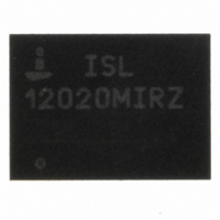
ISL12020MIRZ Intersil, ISL12020MIRZ Datasheet - Page 28

ISL12020MIRZ
Manufacturer Part Number
ISL12020MIRZ
Description
IC RTC/CALENDAR TEMP SNSR 20-DFN
Manufacturer
Intersil
Type
Clock/Calendarr
Datasheet
1.ISL12020MIRZ-T.pdf
(32 pages)
Specifications of ISL12020MIRZ
Memory Size
1K (128 x 8)
Time Format
HH:MM:SS (12/24 hr)
Date Format
YY-MM-DD-dd
Interface
I²C, 2-Wire Serial
Voltage - Supply
2.7 V ~ 5.5 V
Operating Temperature
-40°C ~ 85°C
Mounting Type
Surface Mount
Package / Case
20-DFN
Lead Free Status / RoHS Status
Lead free / RoHS Compliant
Available stocks
Company
Part Number
Manufacturer
Quantity
Price
Company:
Part Number:
ISL12020MIRZ
Manufacturer:
Intersil
Quantity:
454
Part Number:
ISL12020MIRZ
Manufacturer:
INTERSIL
Quantity:
20 000
Part Number:
ISL12020MIRZ-T
Manufacturer:
INTERSIL
Quantity:
20 000
.
The diode, D
voltage but will protect the circuit should battery voltage
drop below 1.8V. The jumper is added as a safeguard
should the battery ever need to be disconnect from the
circuit.
The V
the data sheet spec (10V/ms) otherwise battery
switchover can be delayed, resulting in SRAM contents
corruption and oscillator operation interruption.
Some applications will require separate supplies for the
RTC V
may compromise the operation of the I
applications that do require serial bus communication
with the RTC V
pulled low during the time the RTC V
0V. Otherwise, the device may lose serial bus
communications once V
to normal operation ONLY once V
powered down together.
Layout Considerations
The ISL12020M contains a quarts crystal and requires
special handling during PC board assembly. Excessive
shock and vibrations should be avoided. Ultrasound
cleaning is not advisable. See Note 7 on page 5 in the
electrical specifications table pertaining to solder reflow
effects on oscillator accuracy.
The crystal pins X1 and X2 have a very high impedance,
and oscillator circuits operating at low frequencies (such
as 32.768kHz) are known to pick up noise very easily if
layout precautions are not followed. Most instances of
erratic clocking or large accuracy errors can be traced to
the susceptibility of the oscillator circuit to interference
from adjacent high speed clock or data lines. Careful
layout of the RTC circuit will avoid noise pickup and
insure accurate clocking.
Figure 21 shows a suggested layout for the ISL12020M
device. Three main precautions should be followed:
1. Do not run the serial bus lines or any high speed logic
2. Add a ground trace around the device with one end
3. Do not run a ground or power plane immediately
FIGURE 20. SUGGESTED BATTERY-BACKUP CIRCUIT
V
0.1µF
DD
TO 5.5V
lines in the vicinity of the X1 and X2 pins. These logic
level lines can induce noise in the oscillator circuit,
causing misclocking.
terminated at the chip ground. This guard ring will
provide termination for emitted noise in the vicinity
of the RTC device.
under the RTC. This will add capacitance to the
C
= 2.7V
IN
DD
DD
negative slew rate should be limited to below
and the I
BAT
VDD
ISL12020M
DD
will add a small drop to the battery
GND
powered down, the SDA pin must be
2
C pullups. This is not advised, as it
VBAT
DD
28
is powered up, and will return
J
BAT
DD
BAT43W
C
0.1µF
DD
and V
D
BAT
BAT
2
ramps down to
C bus. For
BAT
+
V
are both
BAT
TO 3.2V
ISL12020M
= 1.8V
.
The best way to run clock lines around the RTC is to stay
outside of the ground ring by at least a few millimeters.
Also, use the V
they can isolate clock lines from the X1 and X2 pins. In
addition, if the IRQ/F
be routed away from the RTC device as well.
Measuring Oscillator Accuracy
The best way to analyze the ISL12020M frequency
accuracy is to set the IRQ/F
frequency, and look at the output of that pin on a high
accuracy frequency counter (at least 7 digits accuracy).
Note that the IRQ/F
require a pull-up resistor.
Using the 1.0Hz output frequency is the most convenient
as the ppm error is just as shown in Equation 7:
Other frequencies may be used for measurement but the
error calculation becomes more complex.
When the proper layout guidelines above are observed,
the oscillator should start-up in most circuits in less than
one second. When testing RTC circuits, a common
impulse is to apply a scope probe to the circuit at the X2
pin (oscillator output) and observe the waveform. DO
NOT DO THIS! Although in some cases you may see a
usable waveform, due to the parasitics (usually 10pF to
ground) applied with the scope probe, there will be no
useful information in that waveform other than the fact
that the circuit is oscillating. The X2 output is sensitive to
capacitive impedance so the voltage levels and the
frequency will be affected by the parasitic elements in
the scope probe. Use the F
counter for the most accurate results.
ppm error
FIGURE 21. SUGGESTED LAYOUT FOR ISL12020M
X1/X2 pins and change the trimmed frequency of
the oscillator. Instead, try to leave a gap in any
planes under the RTC device.
=
(
F
OUT
BAT
–
1
and V
)
OUT
×
OUT
1e6
is an drain output and will
DD
pin is used as a clock, it should
OUT
OUT
as guard ring lines as well,
output and a frequency
pin for a specific
February 11, 2010
GROUND
RING
(EQ. 7)
FN6667.4
F
SCL
SDA
OUT


