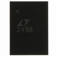
LTC2498IUHF#PBF Linear Technology, LTC2498IUHF#PBF Datasheet - Page 14

LTC2498IUHF#PBF
Manufacturer Part Number
LTC2498IUHF#PBF
Description
IC ADC 24BIT 16CH 38-QFN
Manufacturer
Linear Technology
Datasheet
1.LTC2498CUHFPBF.pdf
(38 pages)
Specifications of LTC2498IUHF#PBF
Number Of Bits
24
Sampling Rate (per Second)
7.5
Data Interface
MICROWIRE™, Serial, SPI™
Number Of Converters
1
Power Dissipation (max)
480µW
Voltage Supply Source
Single Supply
Operating Temperature
-40°C ~ 85°C
Mounting Type
Surface Mount
Package / Case
38-WFQFN, Exposed Pad
Number Of Elements
1
Resolution
24Bit
Architecture
Delta-Sigma
Sample Rate
0.008KSPS
Input Polarity
Bipolar
Input Type
Voltage
Rated Input Volt
±2.75V
Differential Input
Yes
Power Supply Requirement
Single
Single Supply Voltage (typ)
3.3/5V
Single Supply Voltage (min)
2.7V
Single Supply Voltage (max)
5.5V
Dual Supply Voltage (typ)
Not RequiredV
Dual Supply Voltage (min)
Not RequiredV
Dual Supply Voltage (max)
Not RequiredV
Integral Nonlinearity Error
10ppm of Vref
Operating Temp Range
-40C to 85C
Operating Temperature Classification
Industrial
Mounting
Surface Mount
Pin Count
38
Package Type
QFN EP
Lead Free Status / RoHS Status
Lead free / RoHS Compliant
Available stocks
Company
Part Number
Manufacturer
Quantity
Price
applications inForMation
LTC2498
CONVERTER OPERATION
Converter Operation Cycle
The LTC2498 is a multi-channel, low power, delta-sigma
analog-to-digital converter with an easy to use 4-wire inter-
face and automatic differential input current cancellation.
Its operation is made up of three states (See Figure 2).
The converter operating cycle begins with the conver-
sion, followed by the sleep state and ends with the data
input/output cycle. The 4-wire interface consists of serial
data output (SDO), serial clock (SCK), chip select (CS)
and serial data input (SDI).The interface, timing, operation
cycle, and data output format is compatible with Linear’s
entire family of ΔS converters.
Initially, at power-up, the LTC2498 performs a conversion.
Once the conversion is complete, the device enters the
sleep state. While in this sleep state, if CS in HIGH, power
consumption is reduced by two orders of magnitude. The
part remains in the sleep state as long as CS is HIGH. The
conversion result is held indefinitely in a static shift register
while the part is in the sleep state.
Once CS is pulled LOW, the device powers up, exits the
sleep mode, and enters the data input/output state. If CS
is brought HIGH before the first rising edge of SCK, the
device returns to the sleep state and the power is reduced.
If CS is brought HIGH after the first rising edge of SCK, the
Figure 2. LTC2498 State Transition Diagram
CONFIGURATION SELECT
IN
CHANNEL SELECT
+
DATA OUTPUT
= CH0, IN
50/60Hz,1X
POWER UP
CONVERT
CS = LOW
SCK
SLEEP
AND
–
= CH1
2498 F02
data output cycle is aborted and a new conversion cycle
begins. The data output corresponds to the conversion
just completed. This result is shifted out on the serial data
output pin (SDO) under the control of the serial clock pin
(SCK). Data is updated on the falling edge of SCK allowing
the user to reliably latch data on the rising edge of SCK (See
Figure 3). The configuration data for the next conversion
is also loaded into the device at this time. Data is loaded
from the serial data input pin (SDI) on each rising edge
of SCK. The data input/output cycle is concluded once 32
bits are read out of the ADC or when CS is brought HIGH.
The device automatically initiates a new conversion and
the cycle repeats.
Through timing control of the CS and SCK pins, the LTC2498
offers several flexible modes of operation (internal or
external SCK and free-running conversion modes). These
various modes do not require programming and do not
disturb the cyclic operation described above. These modes
of operation are described in detail in the Serial Interface
Timing Modes section.
Ease of Use
The LTC2498 data output has no latency, filter settling
delay or redundant data associated with the conversion
cycle. There is a one-to-one correspondence between the
conversion and the output data. Therefore, multiplexing
multiple analog inputs is straightforward. Each conver-
sion, immediately following a newly selected input or
mode, is valid and accurate to the full specifications of
the device.
The LTC2498 automatically performs offset and full scale
calibration every conversion cycle independent of the
input channel selected. This calibration is transparent to
the user and has no effect with the operation cycle de-
scribed above. The advantage of continuous calibration
is extreme stability of offset and full-scale readings with
respect to time, supply voltage variation, input channel,
and temperature drift.
Easy Drive Input Current Cancellation
The LTC2498 combines a high precision delta-sigma ADC
with an automatic, differential, input current cancellation
front end. A proprietary front end passive sampling network
2498fe


