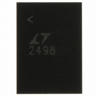
LTC2498IUHF#PBF Linear Technology, LTC2498IUHF#PBF Datasheet - Page 22

LTC2498IUHF#PBF
Manufacturer Part Number
LTC2498IUHF#PBF
Description
IC ADC 24BIT 16CH 38-QFN
Manufacturer
Linear Technology
Datasheet
1.LTC2498CUHFPBF.pdf
(38 pages)
Specifications of LTC2498IUHF#PBF
Number Of Bits
24
Sampling Rate (per Second)
7.5
Data Interface
MICROWIRE™, Serial, SPI™
Number Of Converters
1
Power Dissipation (max)
480µW
Voltage Supply Source
Single Supply
Operating Temperature
-40°C ~ 85°C
Mounting Type
Surface Mount
Package / Case
38-WFQFN, Exposed Pad
Number Of Elements
1
Resolution
24Bit
Architecture
Delta-Sigma
Sample Rate
0.008KSPS
Input Polarity
Bipolar
Input Type
Voltage
Rated Input Volt
±2.75V
Differential Input
Yes
Power Supply Requirement
Single
Single Supply Voltage (typ)
3.3/5V
Single Supply Voltage (min)
2.7V
Single Supply Voltage (max)
5.5V
Dual Supply Voltage (typ)
Not RequiredV
Dual Supply Voltage (min)
Not RequiredV
Dual Supply Voltage (max)
Not RequiredV
Integral Nonlinearity Error
10ppm of Vref
Operating Temp Range
-40C to 85C
Operating Temperature Classification
Industrial
Mounting
Surface Mount
Pin Count
38
Package Type
QFN EP
Lead Free Status / RoHS Status
Lead free / RoHS Compliant
Available stocks
Company
Part Number
Manufacturer
Quantity
Price
applications inForMation
LTC2498
External Serial Clock, Single Cycle Operation
This timing mode uses an external serial clock to shift out
the conversion result and CS to monitor and control the
state of the conversion cycle, see Figure 6.
The external serial clock mode is selected during the power-
up sequence and on each falling edge of CS. In order to
enter and remain in the external SCK mode of operation,
SCK must be driven LOW both at power-up and on each
CS falling edge. If SCK is HIGH on the falling edge of CS,
the device will switch to the internal SCK mode.
The serial data output pin (SDO) is Hi-Z as long as CS is
HIGH. At any time during the conversion cycle, CS may be
pulled LOW in order to monitor the state of the converter.
While CS is LOW, EOC is output to the SDO pin.
EOC = 1 while a conversion is in progress and EOC = 0 if
the conversion is complete and the device is in the sleep
state. Independent of CS, the device automatically enters
the sleep state once the conversion is complete; however,
in order to reduce the power, CS must be HIGH.
(EXTERNAL)
SDO
SCK
SDI
CS
CONVERSION
DON'T CARE
SLEEP
Hi-Z
BIT 31
1
EOC
1
BIT 30
Figure 6. External Serial Clock, Single Cycle Operation
“0”
0
2
10µF
2.7V TO 5.5V
BIT 29
SIG
EN
3
0.1V TO V
REFERENCE
0.1µF
ANALOG
BIT 28 BIT 27 BIT 26 BIT 25 BIT 24 BIT 23 BIT 22 BIT 21
INPUTS
VOLTAGE
MSB
SGL
4
CC
ODD
5
•
•
•
•
•
•
28
29
30
15
16
23
8
7
V
REF
REF
CH0
CH7
CH8
CH15
COM
A2
CC
•
•
•
•
•
•
6
LTC2498
+
–
A1
7
SDO
GND
SCK
SDI
CS
f
DATA INPUT/OUTPUT
O
When the device is in the sleep state, its conversion result
is held in an internal static shift register. The device remains
in the sleep state until the first rising edge of SCK is seen
while CS is LOW. The input data is then shifted in via the
SDI pin on each rising edge of SCK (including the first rising
edge). The channel selection and converter configuration
mode will be used for the following conversion cycle. If
the input channel or converter configuration is changed
during this I/O cycle, the new settings take effect on the
conversion cycle following the data input/output cycle.
The output data is shifted out the SDO pin on each falling
edge of SCK. This enables external circuitry to latch the
output on the rising edge of SCK. EOC can be latched on
the first rising edge of SCK and the last bit of the conver-
sion result can be latched on the 32nd rising edge of SCK.
On the 32nd falling edge of SCK, the device begins a new
conversion and SDO goes HIGH (EOC = 1) indicating a
conversion is in progress.
At the conclusion of the data cycle, CS may remain LOW
and EOC monitored as an end-of-conversion interrupt.
1,3,4,5,6,31,32,33,39
A0
34
38
35
37
36
8
EN2
9
4-WIRE
SPI INTERFACE
= EXTERNAL OSCILLATOR
= INTERNAL OSCILLATOR
IM
10
FA
11
BIT 20 BIT 19
FB
12
SPD
13
BIT 18 BIT 17
14
DON'T CARE
BIT 0
32
CONVERSION
Hi-Z
2498fe
2498 F06


