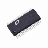
LTC1608CG#PBF Linear Technology, LTC1608CG#PBF Datasheet - Page 11

LTC1608CG#PBF
Manufacturer Part Number
LTC1608CG#PBF
Description
IC A/D CONV 16BIT SAMPLNG 36SSOP
Manufacturer
Linear Technology
Datasheet
1.LTC1608CGPBF.pdf
(20 pages)
Specifications of LTC1608CG#PBF
Number Of Bits
16
Sampling Rate (per Second)
500k
Data Interface
Parallel
Number Of Converters
1
Power Dissipation (max)
420mW
Voltage Supply Source
Analog and Digital, Dual ±
Operating Temperature
0°C ~ 70°C
Mounting Type
Surface Mount
Package / Case
36-SSOP (0.200", 5.30mm Width)
Number Of Elements
1
Resolution
16Bit
Architecture
SAR
Sample Rate
500KSPS
Input Polarity
Bipolar
Input Type
Voltage
Rated Input Volt
±2.5V
Differential Input
Yes
Power Supply Requirement
Dual
Single Supply Voltage (typ)
Not RequiredV
Single Supply Voltage (min)
Not RequiredV
Single Supply Voltage (max)
Not RequiredV
Dual Supply Voltage (typ)
±5V
Dual Supply Voltage (min)
±4.75V
Dual Supply Voltage (max)
±5.25V
Power Dissipation
420mW
Integral Nonlinearity Error
±4LSB
Operating Temp Range
0C to 70C
Operating Temperature Classification
Commercial
Mounting
Surface Mount
Pin Count
36
Package Type
SSOP
Resolution (bits)
16bit
Sampling Rate
500kSPS
Input Channel Type
Differential
Supply Voltage Range - Analogue
± 4.75V To ± 5.25V
Supply Voltage Range - Digital
4.75V To
Rohs Compliant
Yes
Lead Free Status / RoHS Status
Lead free / RoHS Compliant
Available stocks
Company
Part Number
Manufacturer
Quantity
Price
APPLICATIO S I FOR ATIO
spike while charging the sample-and-hold capacitors at
the end of conversion. During conversion, the analog
inputs draw only a small leakage current. If the source
impedance of the driving circuit is low, then the LTC1608
inputs can be driven directly. As source impedance in-
creases so will acquisition time (see Figure 10). For
minimum acquisition time with high source impedance, a
buffer amplifier should be used. The only requirement is
that the amplifier driving the analog input(s) must settle
after the small current spike before the next conversion
starts (settling time must be 200ns for full throughput
rate).
Choosing an Input Amplifier
Choosing an input amplifier is easy if a few requirements
are taken into consideration. First, to limit the magnitude
of the voltage spike seen by the amplifier from charging
the sampling capacitor, choose an amplifier that has a
low output impedance (< 100 ) at the closed-loop band-
width frequency. For example, if an amplifier is used in a
gain of +1 and has a unity-gain bandwidth of 50MHz, then
RD = CONVST
RD = CONVST
CS = 0
BUSY
DATA
U
CS = 0
BUSY
DATA
U
t
6
t
10
t
6
W
t
10
DATA (N – 1)
D15 TO D0
Figure 8. Mode 2. Slow Memory Mode Timing
t
CONV
DATA (N – 1)
D15 TO D0
t
CONV
U
t
11
Figure 9. ROM Mode Timing
t
7
D15 TO D0
DATA N
t
11
the output impedance at 50MHz should be less than
100 . The second requirement is that the closed-loop
bandwidth must be greater than 15MHz to ensure
adequate small-signal settling for full throughput rate. If
slower op amps are used, more settling time can be
provided by increasing the time between conversions.
t
t
8
8
0.01
0.1
10
Figure 10. t
1
1
D15 TO D0
DATA N
D15 TO D0
10
SOURCE RESISTANCE ( )
DATA N
ACQ
vs Source Resistance
100
DATA (N + 1)
D15 TO D0
1k
1608 F09
1608 F10
LTC1608
1608 F08
10k
11


