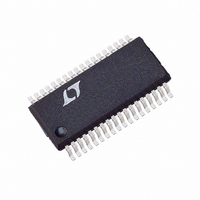
LTC1608CG#PBF Linear Technology, LTC1608CG#PBF Datasheet - Page 6

LTC1608CG#PBF
Manufacturer Part Number
LTC1608CG#PBF
Description
IC A/D CONV 16BIT SAMPLNG 36SSOP
Manufacturer
Linear Technology
Datasheet
1.LTC1608CGPBF.pdf
(20 pages)
Specifications of LTC1608CG#PBF
Number Of Bits
16
Sampling Rate (per Second)
500k
Data Interface
Parallel
Number Of Converters
1
Power Dissipation (max)
420mW
Voltage Supply Source
Analog and Digital, Dual ±
Operating Temperature
0°C ~ 70°C
Mounting Type
Surface Mount
Package / Case
36-SSOP (0.200", 5.30mm Width)
Number Of Elements
1
Resolution
16Bit
Architecture
SAR
Sample Rate
500KSPS
Input Polarity
Bipolar
Input Type
Voltage
Rated Input Volt
±2.5V
Differential Input
Yes
Power Supply Requirement
Dual
Single Supply Voltage (typ)
Not RequiredV
Single Supply Voltage (min)
Not RequiredV
Single Supply Voltage (max)
Not RequiredV
Dual Supply Voltage (typ)
±5V
Dual Supply Voltage (min)
±4.75V
Dual Supply Voltage (max)
±5.25V
Power Dissipation
420mW
Integral Nonlinearity Error
±4LSB
Operating Temp Range
0C to 70C
Operating Temperature Classification
Commercial
Mounting
Surface Mount
Pin Count
36
Package Type
SSOP
Resolution (bits)
16bit
Sampling Rate
500kSPS
Input Channel Type
Differential
Supply Voltage Range - Analogue
± 4.75V To ± 5.25V
Supply Voltage Range - Digital
4.75V To
Rohs Compliant
Yes
Lead Free Status / RoHS Status
Lead free / RoHS Compliant
Available stocks
Company
Part Number
Manufacturer
Quantity
Price
LTC1608
TYPICAL PERFOR A CE CHARACTERISTICS
PI FU CTIO S
A
difference voltage between A
tial range of 2.5V. A
A
A
to a DC voltage or driven differentially with A
V
2.2 F tantalum in parallel with 0.1 F ceramic.
REFCOMP (Pin 4): 4.375V (Nominal) Reference Compen-
sation Pin. Bypass to AGND with 22 F tantalum in parallel
with 0.1 F ceramic. This is not recommended for use as
an external reference due to part-to-part output voltage
variations and glitches that occur during the conversion.
AGND (Pins 5 to 8): Analog Grounds. Tie to analog ground
plane.
DV
with 10 F tantalum in parallel with 0.1 F ceramic.
DGND (Pin 10): Digital Ground for Internal Logic. Tie to
analog ground plane.
D15 to D0 (Pins 11 to 26): Three-State Data Outputs. D15
is the Most Significant Bit.
BUSY (Pin 27): The BUSY output shows the converter
status. It is low when a conversion is in progress. Data is
valid on the rising edge of BUSY.
6
IN
IN
IN
REF
–100
–120
–140
–20
–40
–60
–80
DD
U
+
–
–
0
(Pin 1): Positive Analog Input. The ADC converts the
(Pin 2): Negative Analog Input. Can be grounded, tied
0
(Pin 3): 2.5V Reference Output. Bypass to AGND with
is grounded.
Intermodulation Distortion
(Pin 9): 5V Digital Power Supply. Bypass to DGND
U
50
FREQUENCY (kHz)
100
U
IN
150
f
f
f
SAMPLE
IN1
IN2
+
has a 2.5V input range when
= 96.56kHz
= 99.98kHz
W
200
IN
= 500kHz
+
1608 G07
and A
U
250
IN
–
with a differen-
–100
–120
–140
–20
–40
–60
–80
0
IN
1k
Power Supply Feedthrough
vs Ripple Frequency
+
f
V
SAMPLE
.
RIPPLE
= 10mV
= 500kHz
INPUT FREQUENCY (Hz)
A
10k
VDD
OGND (Pin 28): Digital Ground for Output Drivers.
OV
Bypass to OGND with 10 F tantalum in parallel with 0.1 F
ceramic.
RD (Pin 30): Read Input. A logic low enables the output
drivers when CS is low.
CONVST (Pin 31): Conversion Start Signal. This active
low signal starts a conversion on its falling edge when CS
is low.
CS (Pin 32): The Chip Select Input. Must be low for the ADC
to recognize CONVST and RD inputs.
SHDN (Pin 33): Power Shutdown. Drive this pin low with
CS low for nap mode. Drive this pin low with CS high for
sleep mode.
V
10 F tantalum in parallel with 0.1 F ceramic.
AV
with 10 F tantalum in parallel with 0.1 F ceramic.
AV
with 10 F tantalum in parallel with 0.1 F ceramic and
connect this pin to Pin 35 with a 10 resistor.
SS
DD
DD
DD
(Pin 34): – 5V Negative Supply. Bypass to AGND with
100k
V
SS
(Pin 35): 5V Analog Power Supply. Bypass to AGND
(Pin 36): 5V Analog Power Supply. Bypass to AGND
(Pin 29): Digital Power Supply for Output Drivers.
1608 G08
1M
80
70
60
50
40
30
20
10
0
1k
Input Common Mode Rejection
vs Input Frequency
INPUT FREQUENCY (Hz)
10k
100k
1608 G14a
1M


