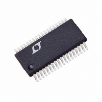
LTC1608CG#PBF Linear Technology, LTC1608CG#PBF Datasheet - Page 4

LTC1608CG#PBF
Manufacturer Part Number
LTC1608CG#PBF
Description
IC A/D CONV 16BIT SAMPLNG 36SSOP
Manufacturer
Linear Technology
Datasheet
1.LTC1608CGPBF.pdf
(20 pages)
Specifications of LTC1608CG#PBF
Number Of Bits
16
Sampling Rate (per Second)
500k
Data Interface
Parallel
Number Of Converters
1
Power Dissipation (max)
420mW
Voltage Supply Source
Analog and Digital, Dual ±
Operating Temperature
0°C ~ 70°C
Mounting Type
Surface Mount
Package / Case
36-SSOP (0.200", 5.30mm Width)
Number Of Elements
1
Resolution
16Bit
Architecture
SAR
Sample Rate
500KSPS
Input Polarity
Bipolar
Input Type
Voltage
Rated Input Volt
±2.5V
Differential Input
Yes
Power Supply Requirement
Dual
Single Supply Voltage (typ)
Not RequiredV
Single Supply Voltage (min)
Not RequiredV
Single Supply Voltage (max)
Not RequiredV
Dual Supply Voltage (typ)
±5V
Dual Supply Voltage (min)
±4.75V
Dual Supply Voltage (max)
±5.25V
Power Dissipation
420mW
Integral Nonlinearity Error
±4LSB
Operating Temp Range
0C to 70C
Operating Temperature Classification
Commercial
Mounting
Surface Mount
Pin Count
36
Package Type
SSOP
Resolution (bits)
16bit
Sampling Rate
500kSPS
Input Channel Type
Differential
Supply Voltage Range - Analogue
± 4.75V To ± 5.25V
Supply Voltage Range - Digital
4.75V To
Rohs Compliant
Yes
Lead Free Status / RoHS Status
Lead free / RoHS Compliant
Available stocks
Company
Part Number
Manufacturer
Quantity
Price
POWER REQUIRE E TS
LTC1608
otherwise specifications are at T
SYMBOL
V
V
I
I
P
otherwise specifications are at T
SYMBOL
f
t
t
t
t
t
t
t
t
t
t
t
t
t
t
t
t
t
Note 1: Absolute Maximum Ratings are those values beyond which the life
of a device may be impaired.
Note 2: All voltage values are with respect to ground with DGND, OGND
and AGND wired together unless otherwise noted.
TI I G CHARACTERISTICS
4
DD
SS
SMPL(MAX)
CONV
ACQ
ACQ+CONV(MIN)
1
2
3
4
5
6
7
8
9
10
11
12
13
14
DD
SS
D
W
U
PARAMETER
Positive Supply Voltage
Negative Supply Voltage
Positive Supply Current
Negative Supply Current
Power Dissipation
PARAMETER
Maximum Sampling Frequency
Conversion Time
Acquisition Time
Throughput Time (Acquisition + Conversion)
CS to RD Setup Time
CS to CONVST Setup Time
SHDN to CS Setup Time
SHDN to CONVST Wake-Up Time
CONVST Low Time
CONVST to BUSY Delay
Data Ready Before BUSY
Delay Between Conversions
Wait Time RD After BUSY
Data Access Time After RD
Bus Relinquish Time
RD Low Time
CONVST High Time
Aperture Delay of Sample-and-Hold
Nap Mode
Sleep Mode
Nap Mode
Sleep Mode
Nap Mode
Sleep Mode
A
A
W U
= 25 C. (Note 5)
= 25 C. (Note 5)
The
The
denotes specifications that apply over the full operating temperature range,
(Notes 12, 13)
CONDITIONS
(Note 12)
CS = RD = 0V
CS = RD = 0V
CS = RD = 0V
CONDITIONS
(Notes 11, 14)
(Notes 11, 12, 15)
(Notes 11, 12)
(Notes 11, 12)
CS = Low (Note 12)
(Note 12)
C
(Note 12)
(Note 12)
C
C
(Note 12)
(Note 12)
L
L
L
denotes specifications that apply over the full operating temperature range,
= 25pF
= 25pF
= 100pF (Note 11)
CS = 0V, SHDN = 0V
CS = 5V, SHDN = 0V
CS = 0V, SHDN = 0V
CS = 5V, SHDN = 0V
CS = 0V, SHDN = 0V
CS = 5V, SHDN = 0V
Note 3: When these pin voltages are taken below V
will be clamped by internal diodes. This product can handle input currents
greater than 100mA below V
SS
or above V
– 4.75
4.75
MIN
MIN
500
200
1.0
– 5
t
10
10
40
32
40
0
10
DD
without latchup.
0.01
1.45
1.67
TYP
270
TYP
600
400
1.5
7.5
22
32
36
60
25
45
30
1
1
1
2
SS
or above V
– 5.25
MAX
MAX
5.25
420
100
100
100
400
2.4
1.8
35
49
12
80
40
50
60
75
50
60
1
2
DD
, they
UNITS
UNITS
mW
mW
mW
kHz
mA
mA
mA
ns
ns
ns
ns
ns
ns
ns
ns
ns
ns
ns
ns
ns
ns
ns
ns
ns
ns
ns
ns
ns
V
V
A
A
A
s
s


