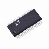
LTC1608CG#PBF Linear Technology, LTC1608CG#PBF Datasheet - Page 7

LTC1608CG#PBF
Manufacturer Part Number
LTC1608CG#PBF
Description
IC A/D CONV 16BIT SAMPLNG 36SSOP
Manufacturer
Linear Technology
Datasheet
1.LTC1608CGPBF.pdf
(20 pages)
Specifications of LTC1608CG#PBF
Number Of Bits
16
Sampling Rate (per Second)
500k
Data Interface
Parallel
Number Of Converters
1
Power Dissipation (max)
420mW
Voltage Supply Source
Analog and Digital, Dual ±
Operating Temperature
0°C ~ 70°C
Mounting Type
Surface Mount
Package / Case
36-SSOP (0.200", 5.30mm Width)
Number Of Elements
1
Resolution
16Bit
Architecture
SAR
Sample Rate
500KSPS
Input Polarity
Bipolar
Input Type
Voltage
Rated Input Volt
±2.5V
Differential Input
Yes
Power Supply Requirement
Dual
Single Supply Voltage (typ)
Not RequiredV
Single Supply Voltage (min)
Not RequiredV
Single Supply Voltage (max)
Not RequiredV
Dual Supply Voltage (typ)
±5V
Dual Supply Voltage (min)
±4.75V
Dual Supply Voltage (max)
±5.25V
Power Dissipation
420mW
Integral Nonlinearity Error
±4LSB
Operating Temp Range
0C to 70C
Operating Temperature Classification
Commercial
Mounting
Surface Mount
Pin Count
36
Package Type
SSOP
Resolution (bits)
16bit
Sampling Rate
500kSPS
Input Channel Type
Differential
Supply Voltage Range - Analogue
± 4.75V To ± 5.25V
Supply Voltage Range - Digital
4.75V To
Rohs Compliant
Yes
Lead Free Status / RoHS Status
Lead free / RoHS Compliant
Available stocks
Company
Part Number
Manufacturer
Quantity
Price
APPLICATIO S I FOR ATIO
FU CTIO AL BLOCK DIAGRA
TEST CIRCUITS
CONVERSION DETAILS
The LTC1608 uses a successive approximation algorithm
and internal sample-and-hold circuit to convert an analog
signal to a 16-bit parallel output. The ADC is complete with
a sample-and-hold, a precision reference and an internal
clock. The control logic provides easy interface to micro-
processors and DSPs. (Please refer to the Digital Interface
section for the data format.)
Conversion start is controlled by the CS and CONVST
inputs. At the start of the conversion, the successive
approximation register (SAR) resets. Once a conversion
cycle has begun, it cannot be restarted.
U
(A) Hi-Z TO V OH AND V OL TO V OH
DN
U
Load Circuits for Access Timing
1k
U
ANALOG INPUT
DIFFERENTIAL
C
L
22 F
U
2.5V
+
(B) Hi-Z TO V OL AND V OH TO V OL
4
2
1
REFCOMP
A
A
DN
IN
IN
W
–
+
3
V
2.2 F
4.375V
REF
5V
+
–
1k
AGND
C
L
SAMPLING
1.75X
5
16-BIT
10 F
ADC
U
1608 TC01
AGND
+
W
AV
DD
6
36
10
AGND
7.5k
AV
7
B15 TO B0
5V
DD
35
+
2.5V
REF
10 F
AGND
8
During the conversion, the internal differential 16-bit
capacitive DAC output is sequenced by the SAR from the
Most Significant Bit (MSB) to the Least Significant Bit
(LSB). Referring to Figure 1, the A
acquired during the acquire phase and the comparator
offset is nulled by the zeroing switches. In this acquire
phase, a duration of 480ns will provide enough time for the
sample-and-hold capacitors to acquire the analog signal.
During the convert phase, the comparator zeroing switches
open, putting the comparator into compare mode. The
input switches connect the C
transferring the differential analog input charge onto the
summing junctions. This input charge is successively
–5V
V
SS
34
5V
BUFFERS
CONTROL
OUTPUT
DV
9
TIMING
LOGIC
+
+
AND
DD
10 F
10 F
10
DGND
DN
Load Circuits for Output Float Delay
D15 TO D0
(A) V OH TO Hi-Z
CONVST
OGND
SHDN
BUSY
OV
1k
1608 BD
RD
CS
DD
11 TO 26
33
32
31
30
27
29
28
16-BIT
PARALLEL
BUS
C
L
+
CONTROL
LINES
SMPL
P
10 F
DN
5V OR
3V
(B) V OL TO Hi-Z
IN
capacitors to ground,
+
5V
and A
1k
1608 TC02
C
L
LTC1608
IN
–
inputs are
7


