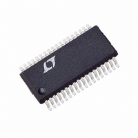
LTC1608CG#PBF Linear Technology, LTC1608CG#PBF Datasheet - Page 3

LTC1608CG#PBF
Manufacturer Part Number
LTC1608CG#PBF
Description
IC A/D CONV 16BIT SAMPLNG 36SSOP
Manufacturer
Linear Technology
Datasheet
1.LTC1608CGPBF.pdf
(20 pages)
Specifications of LTC1608CG#PBF
Number Of Bits
16
Sampling Rate (per Second)
500k
Data Interface
Parallel
Number Of Converters
1
Power Dissipation (max)
420mW
Voltage Supply Source
Analog and Digital, Dual ±
Operating Temperature
0°C ~ 70°C
Mounting Type
Surface Mount
Package / Case
36-SSOP (0.200", 5.30mm Width)
Number Of Elements
1
Resolution
16Bit
Architecture
SAR
Sample Rate
500KSPS
Input Polarity
Bipolar
Input Type
Voltage
Rated Input Volt
±2.5V
Differential Input
Yes
Power Supply Requirement
Dual
Single Supply Voltage (typ)
Not RequiredV
Single Supply Voltage (min)
Not RequiredV
Single Supply Voltage (max)
Not RequiredV
Dual Supply Voltage (typ)
±5V
Dual Supply Voltage (min)
±4.75V
Dual Supply Voltage (max)
±5.25V
Power Dissipation
420mW
Integral Nonlinearity Error
±4LSB
Operating Temp Range
0C to 70C
Operating Temperature Classification
Commercial
Mounting
Surface Mount
Pin Count
36
Package Type
SSOP
Resolution (bits)
16bit
Sampling Rate
500kSPS
Input Channel Type
Differential
Supply Voltage Range - Analogue
± 4.75V To ± 5.25V
Supply Voltage Range - Digital
4.75V To
Rohs Compliant
Yes
Lead Free Status / RoHS Status
Lead free / RoHS Compliant
Available stocks
Company
Part Number
Manufacturer
Quantity
Price
DY A IC ACCURACY
I TER AL REFERE CE CHARACTERISTICS
DIGITAL I PUTS A D DIGITAL OUTPUTS
SYMBOL
V
V
I
C
V
V
I
C
I
I
operating temperature range, otherwise specifications are at T
SYMBOL
S/N
S/(N + D)
THD
SFDR
IMD
PARAMETER
V
V
V
V
REFCOMP Output Voltage
IN
OZ
SOURCE
SINK
U
IH
IL
IN
OH
OL
OZ
REF
REF
REF
REF
Output Voltage
Output Tempco
Line Regulation
Output Resistance
U W
U
PARAMETER
High Level Input Voltage
Low Level Input Voltage
Digital Input Current
Digital Input Capacitance
High Level Output Voltage
Low Level Output Voltage
Hi-Z Output Leakage D15 to D0
Hi-Z Output Capacitance D15 to D0
Output Source Current
Output Sink Current
PARAMETER
Signal-to-Noise Ratio
Signal-to-(Noise + Distortion) Ratio
Total Harmonic Distortion
Up to 5th Harmonic
Spurious Free Dynamic Range
Intermodulation Distortion
Full Power Bandwidth
Full Linear Bandwidth (S/(N + D) 84dB)
U
U
U
T
A
= 25 C (Note 5)
CONDITIONS
V
V
V
V
V
V
V
V
CS High (Note 11)
V
V
CONDITIONS
5kHz Input Signal
100kHz Input Signal
5kHz Input Signal
100kHz Input Signal (Note 10)
5kHz Input Signal
100kHz Input Signal
100kHz Input Signal
f
CONDITIONS
I
I
4.75 V
– 5.25V V
0
I
IN1
OUT
OUT
OUT
DD
DD
IN
DD
DD
DD
DD
OUT
OUT
OUT
= 0V to V
= 29.37kHz, f
= 5.25V
= 4.75V
= 4.75V, I
= 4.75V, I
= 4.75V, I
= 4.75V, I
= 0
= 0
= 0
= 0V to V
= 0V
= V
I
OUT
A
DD
DD
= 25 C. (Note 5)
SS
DD
5.25V
1mA
OUT
OUT
OUT
OUT
DD
– 4.75V
, CS High
IN2
= – 10 A
= – 400 A
= 160 A
= 1.6mA
= 32.446kHz
T
The
A
= 25 C (Note 5)
denotes specifications that apply over the full
2.475
MIN
MIN
MIN
2.4
4.0
2.500
4.375
– 100
0.05
0.10
– 1 0
0.01
0.01
TYP
TYP
– 91
– 88
TYP
350
4.5
7.5
10
90
88
90
84
94
5
5
15
LTC1608
2.515
MAX
MAX
MAX
0.8
0.4
15
1 0
10
ppm/ C
UNITS
UNITS
UNITS
LSB/V
LSB/V
3
MHz
kHz
mA
mA
k
dB
dB
dB
dB
dB
dB
dB
dB
pF
pF
V
V
A
V
V
V
V
A
V
V


