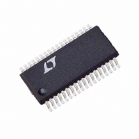
LTC1608CG#PBF Linear Technology, LTC1608CG#PBF Datasheet - Page 17

LTC1608CG#PBF
Manufacturer Part Number
LTC1608CG#PBF
Description
IC A/D CONV 16BIT SAMPLNG 36SSOP
Manufacturer
Linear Technology
Datasheet
1.LTC1608CGPBF.pdf
(20 pages)
Specifications of LTC1608CG#PBF
Number Of Bits
16
Sampling Rate (per Second)
500k
Data Interface
Parallel
Number Of Converters
1
Power Dissipation (max)
420mW
Voltage Supply Source
Analog and Digital, Dual ±
Operating Temperature
0°C ~ 70°C
Mounting Type
Surface Mount
Package / Case
36-SSOP (0.200", 5.30mm Width)
Number Of Elements
1
Resolution
16Bit
Architecture
SAR
Sample Rate
500KSPS
Input Polarity
Bipolar
Input Type
Voltage
Rated Input Volt
±2.5V
Differential Input
Yes
Power Supply Requirement
Dual
Single Supply Voltage (typ)
Not RequiredV
Single Supply Voltage (min)
Not RequiredV
Single Supply Voltage (max)
Not RequiredV
Dual Supply Voltage (typ)
±5V
Dual Supply Voltage (min)
±4.75V
Dual Supply Voltage (max)
±5.25V
Power Dissipation
420mW
Integral Nonlinearity Error
±4LSB
Operating Temp Range
0C to 70C
Operating Temperature Classification
Commercial
Mounting
Surface Mount
Pin Count
36
Package Type
SSOP
Resolution (bits)
16bit
Sampling Rate
500kSPS
Input Channel Type
Differential
Supply Voltage Range - Analogue
± 4.75V To ± 5.25V
Supply Voltage Range - Digital
4.75V To
Rohs Compliant
Yes
Lead Free Status / RoHS Status
Lead free / RoHS Compliant
Available stocks
Company
Part Number
Manufacturer
Quantity
Price
APPLICATIO S I FOR ATIO
Figure 17d. Suggested Evaluation Circuit Board. Inner Layer 1
Showing Separate Analog and Digital Ground Planes
ANALOG GROUND PLANE
Figure 17b. Suggested Evaluation Circuit Board.
Component Side Silkscreen and Signal Traces
Figure 18. Histogram for 4096 Conversions
2500
2000
1500
1000
500
0
–5 –4 –3 –2 –1 0
U
U
CODE
1
2
W
3
DIGITAL GROUND PLANE
4
1608 F18
5
U
noise at the rated throughput. By applying a low distortion
sine wave and analyzing the digital output using an FFT
algorithm, the ADC’s spectral content can be examined for
frequencies outside the fundamental. Figures 19a and 19b
show typical LTC1608 FFT plots.
Signal-to-Noise Ratio
The signal-to-noise plus distortion ratio [S/(N + D)] is the
ratio between the RMS amplitude of the fundamental
input frequency to the RMS amplitude of all other fre-
quency components at the A/D output. The output is band
limited to frequencies from above DC and below half the
sampling frequency. Figure 19a shows a typical spectral
content with a 500kHz sampling rate and a 3kHz input.
Figure 17e. Suggested Evaluation Circuit Board. Inner Layer 2
Showing Separate Analog and Digital Ground Planes
Figure 17c. Suggested Evaluation Circuit Board.
Bottom Side Showing Signal Traces
ANALOG GROUND PLANE
DIGITAL GROUND PLANE
LTC1608
17


