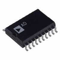
AD7703ARZ Analog Devices Inc, AD7703ARZ Datasheet - Page 11

AD7703ARZ
Manufacturer Part Number
AD7703ARZ
Description
IC ADC 20BIT LC2MOS 20-SOIC
Manufacturer
Analog Devices Inc
Datasheet
1.AD7703AR-REEL.pdf
(16 pages)
Specifications of AD7703ARZ
Data Interface
Serial
Number Of Bits
20
Sampling Rate (per Second)
4k
Number Of Converters
1
Power Dissipation (max)
37mW
Voltage Supply Source
Analog and Digital, Dual ±
Operating Temperature
-40°C ~ 85°C
Mounting Type
Surface Mount
Package / Case
20-SOIC (0.300", 7.50mm Width)
Resolution (bits)
20bit
Sampling Rate
4kSPS
Input Channel Type
Single Ended
Supply Voltage Range - Analog
± 4.5V To ± 5.5V
Supply Current
2.7mA
Number Of Elements
1
Resolution
20Bit
Architecture
Delta-Sigma
Sample Rate
16KSPS
Input Polarity
Unipolar/Bipolar
Input Type
Voltage
Rated Input Volt
2.5/±2.5V
Differential Input
No
Power Supply Requirement
Dual
Single Supply Voltage (typ)
Not RequiredV
Single Supply Voltage (min)
Not RequiredV
Single Supply Voltage (max)
Not RequiredV
Dual Supply Voltage (typ)
±5V
Dual Supply Voltage (min)
±4.5V
Dual Supply Voltage (max)
±5.5V
Power Dissipation
37mW
Differential Linearity Error
±0.5LSB(Typ)
Integral Nonlinearity Error
±0.003%FSR
Operating Temp Range
-40C to 85C
Operating Temperature Classification
Industrial
Mounting
Surface Mount
Pin Count
20
Package Type
SOIC W
Input Signal Type
Single-Ended
Package
20SOIC W
Number Of Analog Inputs
1
Digital Interface Type
Serial (SPI)
Polarity Of Input Voltage
Unipolar|Bipolar
Lead Free Status / RoHS Status
Lead free / RoHS Compliant
Lead Free Status / RoHS Status
Lead free / RoHS Compliant, Lead free / RoHS Compliant
Available stocks
Company
Part Number
Manufacturer
Quantity
Price
Part Number:
AD7703ARZ
Manufacturer:
ADI/亚德诺
Quantity:
20 000
System Calibration
S
(S
S
<(S
In the Bipolar mode, the system offset calibration range is
restricted to ±0.4 V
tions limit the amount of offset that can be calibrated. The span
range of the converter in Bipolar mode is equidistant around the
voltage used for the zero-scale point. When the zero-scale point
is calibrated, it must not cause either of the two endpoints of the
bipolar transfer function to exceed the positive or the negative
input overrange points (+V
the span range is set to a minimum (0.8 V
can move +0.4 V
fer function to exceed the overrange points. Alternatively, if the
span range is set to 2V
than +0.1 V or –0.1 V before an endpoint of the transfer func-
tion exceeds the input overrange limit.
POWER-UP AND CALIBRATION
A calibration cycle must be carried out after power-up to initial-
ize the device to a consistent starting condition and correct
calibration. The CAL pin must be held high for at least four
clock cycles, after which calibration is initiated on the falling
edge of CAL and takes a maximum of 3,145,655 clock cycles
(approximately 768 ms with a 4.096 MHz clock). See Table III.
The type of calibration cycle initiated by CAL is determined by
the SC1 and SC2 inputs, in accordance with Table III.
Drift Considerations
The AD7703 uses chopper stabilization techniques to minimize
input offset drift. Charge injection in the analog switches and
leakage currents at the sampling node are the primary sources of
offset voltage drift in the converter. Figure 13 indicates the typical
offset due to temperature changes after calibration at 25°C. Drift
is relatively flat up to 75°C. Above this temperature, leakage
current becomes the main source of offset drift. Since leakage
current doubles approximately every 10°C, the offset drifts
REV. E
>(S
GAIN
OFF
GAIN
OFF
GAIN
+ 0.5 LSB
– 1.5 LSB
– S
+ 0.5 LSB)
–1.5 LSB)
OFF
)/2 – 0.5 LSB
I
REF
nput Voltage, Unipolar Mode
REF
without causing the endpoints of the trans-
REF
. It should be noted that the span restric-
, the input offset cannot move more
REF
Self-Calibration
>(V
V
(V
V
<(V
+ 0.1) V or (–V
REF
AGND
REF
REF
AGND
– 1.5 LSB
– V
+ 0.5 LSB
– 1.5 LSB)
+ 0.5 LSB)
AGND
REF
)/2 – 0.5 LSB
), the offset voltage
REF
+ 0.1) V. If
Table V. Output Coding
Output Codes
FFFFF
00000
00000
FFFFF
FFFFE
7FFFF
00001
80000
–11–
accordingly. The value of the voltage on the sample capacitor is
updated at a rate determined by the master clock; therefore, the
amount of offset drift that occurs will be proportional to the
elapsed time between samples. Thus, to minimize offset drift at
higher temperatures, higher CLKIN rates are recommended.
Gain drift within the converter depends mainly upon the tem-
perature tracking of the internal capacitors. It is not affected by
leakage currents so it is significantly less than offset drift. The
typical gain drift of the AD7703 is less than 40 LSB over the
specified temperature range.
Measurement errors due to offset drift or gain drift can be
eliminated at any time by recalibrating the converter. Using the
system calibration mode can also minimize offset and gain errors
in the signal conditioning circuitry. Integral and differential
linearity are not significantly affected by temperature changes.
Figure 13. Typical Bipolar Offset vs. Temperature
after Calibration at 25°C
–160
–240
–320
160
–80
80
–55
0
I
Self-Calibration
>(V
V
V
–V
<(–V
nput Voltage, Bipolar Mode
REF
AGND
–35
REF
REF
REF
– 1.5 LSB
+ 0.5 LSB
– 0.5 LSB
–1.5 LSB)
–15
+ 0.5 LSB)
5
TEMPERATURE – C
25
45
System Calibration
>(S
S
S
–S
<(–S
GAIN
OFF
CLKIN = 4.096MHz
GAIN
GAIN
GAIN
– 0.5 LSB
65
– 1.5 LSB
+ 2 S
– 1.5 LSB)
+2 S
85
AD7703
OFF
OFF
105
+ 0.5 LSB
+ 0.5 LSB)
125


