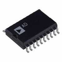
AD7703ARZ Analog Devices Inc, AD7703ARZ Datasheet - Page 5

AD7703ARZ
Manufacturer Part Number
AD7703ARZ
Description
IC ADC 20BIT LC2MOS 20-SOIC
Manufacturer
Analog Devices Inc
Datasheet
1.AD7703AR-REEL.pdf
(16 pages)
Specifications of AD7703ARZ
Data Interface
Serial
Number Of Bits
20
Sampling Rate (per Second)
4k
Number Of Converters
1
Power Dissipation (max)
37mW
Voltage Supply Source
Analog and Digital, Dual ±
Operating Temperature
-40°C ~ 85°C
Mounting Type
Surface Mount
Package / Case
20-SOIC (0.300", 7.50mm Width)
Resolution (bits)
20bit
Sampling Rate
4kSPS
Input Channel Type
Single Ended
Supply Voltage Range - Analog
± 4.5V To ± 5.5V
Supply Current
2.7mA
Number Of Elements
1
Resolution
20Bit
Architecture
Delta-Sigma
Sample Rate
16KSPS
Input Polarity
Unipolar/Bipolar
Input Type
Voltage
Rated Input Volt
2.5/±2.5V
Differential Input
No
Power Supply Requirement
Dual
Single Supply Voltage (typ)
Not RequiredV
Single Supply Voltage (min)
Not RequiredV
Single Supply Voltage (max)
Not RequiredV
Dual Supply Voltage (typ)
±5V
Dual Supply Voltage (min)
±4.5V
Dual Supply Voltage (max)
±5.5V
Power Dissipation
37mW
Differential Linearity Error
±0.5LSB(Typ)
Integral Nonlinearity Error
±0.003%FSR
Operating Temp Range
-40C to 85C
Operating Temperature Classification
Industrial
Mounting
Surface Mount
Pin Count
20
Package Type
SOIC W
Input Signal Type
Single-Ended
Package
20SOIC W
Number Of Analog Inputs
1
Digital Interface Type
Serial (SPI)
Polarity Of Input Voltage
Unipolar|Bipolar
Lead Free Status / RoHS Status
Lead free / RoHS Compliant
Lead Free Status / RoHS Status
Lead free / RoHS Compliant, Lead free / RoHS Compliant
Available stocks
Company
Part Number
Manufacturer
Quantity
Price
Part Number:
AD7703ARZ
Manufacturer:
ADI/亚德诺
Quantity:
20 000
DEFINITION OF TERMS
Linearity Error
This is the maximum deviation of any code from a straight line
passing through the endpoints of the transfer function. The
endpoints of the transfer function are zero-scale (not to be
confused with bipolar zero), a point 0.5 LSB below the first code
transition (000 . . . 000 to 000 . . . 001) and full-scale, a point
1.5 LSB above the last code transition (111 . . . 110 to 111 . . .
111). The error is expressed as a percentage of full scale.
Differential Linearity Error
This is the difference between any code’s actual width and the
ideal (1 LSB) width. Differential linearity error is expressed in
LSB. A differential linearity specification of ± 1 LSB or less
guarantees monotonicity.
Positive Full-Scale Error
Positive full-scale error is the deviation of the last code transition
(111 . . . 110 to 111 . . . 111) from the ideal (V
It applies to both positive and negative analog input ranges and
is expressed in microvolts.
Unipolar Offset Error
Unipolar offset error is the deviation of the first code transition
from the ideal (AGND + 0.5 LSB) when operating in the
Unipolar mode.
Bipolar Zero Error
This is the deviation of the midscale transition (0111 . . . 111 to
1000 . . . 000) from the ideal (AGND – 0.5 LSB) when operating
in the Bipolar mode. It is expressed in microvolts.
Bipolar Negative Full-Scale Error
This is the deviation of the first code transition from the ideal
(–V
REV. E
DRDY
SDATA
SCLK
CS
REF
+ 0.5 LSB) when operating in the Bipolar mode.
HI-Z
Figure 5a. SEC Mode Timing Diagram
Figure 4. SSC Mode Data Hold Time
t
13
DB19
t
11
SDATA
t
CS
12
DB18
t
14
VALID
DATA
t
10
HI-Z
REF
DB1
± 3/2 LSB).
DB0
t
16
HI-Z
–5–
Positive Full-Scale Overrange
Positive full-scale overrange is the amount of overhead available
to handle input voltages greater than +V
peaks or excess voltages due to system gain errors in system
calibration routines) without introducing errors due to overloading
the analog modulator or overflowing the digital filter.
Negative Full-Scale Overrange
This is the amount of overhead available to handle voltages below
–V
the digital filter. Note that the analog input will accept negative
voltage peaks even in the Unipolar mode.
Offset Calibration Range
In the system calibration modes (SC2 low), the AD7703 calibrates
its offset with respect to the A
specification defines the range of voltages, expressed as a
percentage of V
calibrate offset.
Full-Scale Calibration Range
This is the range of voltages that the AD7703 can accept in the
system calibration mode and still correctly calibrate full scale.
Input Span
In system calibration schemes, two voltages applied in sequence
to the AD7703’s analog input define the analog input range. The
input span specification defines the minimum and maximum
input voltages from zero to full scale that the AD7703 can accept
and still accurately calibrate gain. The input span is expressed
as a percentage of V
CLKIN
SDATA
SCLK
REF
CS
without overloading the analog modulator or overflowing
HI-Z
HI-Z
t
Figure 5b. SEC Mode Data Hold Time
Figure 6. SSC Mode Timing Diagram
4
REF
t
DB19
8
, that the AD7703 can accept and still accurately
t
7
SDATA
REF.
CS
t
8
DB18
t
5
VALID
DATA
IN
pin. The offset calibration range
t
15
HI-Z
REF
DB1
(for example, noise
AD7703
DB0
t
9
HI-Z
HI-Z


