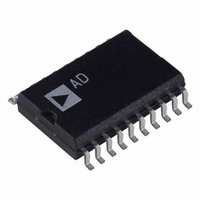
AD7703ARZ Analog Devices Inc, AD7703ARZ Datasheet - Page 13

AD7703ARZ
Manufacturer Part Number
AD7703ARZ
Description
IC ADC 20BIT LC2MOS 20-SOIC
Manufacturer
Analog Devices Inc
Datasheet
1.AD7703AR-REEL.pdf
(16 pages)
Specifications of AD7703ARZ
Data Interface
Serial
Number Of Bits
20
Sampling Rate (per Second)
4k
Number Of Converters
1
Power Dissipation (max)
37mW
Voltage Supply Source
Analog and Digital, Dual ±
Operating Temperature
-40°C ~ 85°C
Mounting Type
Surface Mount
Package / Case
20-SOIC (0.300", 7.50mm Width)
Resolution (bits)
20bit
Sampling Rate
4kSPS
Input Channel Type
Single Ended
Supply Voltage Range - Analog
± 4.5V To ± 5.5V
Supply Current
2.7mA
Number Of Elements
1
Resolution
20Bit
Architecture
Delta-Sigma
Sample Rate
16KSPS
Input Polarity
Unipolar/Bipolar
Input Type
Voltage
Rated Input Volt
2.5/±2.5V
Differential Input
No
Power Supply Requirement
Dual
Single Supply Voltage (typ)
Not RequiredV
Single Supply Voltage (min)
Not RequiredV
Single Supply Voltage (max)
Not RequiredV
Dual Supply Voltage (typ)
±5V
Dual Supply Voltage (min)
±4.5V
Dual Supply Voltage (max)
±5.5V
Power Dissipation
37mW
Differential Linearity Error
±0.5LSB(Typ)
Integral Nonlinearity Error
±0.003%FSR
Operating Temp Range
-40C to 85C
Operating Temperature Classification
Industrial
Mounting
Surface Mount
Pin Count
20
Package Type
SOIC W
Input Signal Type
Single-Ended
Package
20SOIC W
Number Of Analog Inputs
1
Digital Interface Type
Serial (SPI)
Polarity Of Input Voltage
Unipolar|Bipolar
Lead Free Status / RoHS Status
Lead free / RoHS Compliant
Lead Free Status / RoHS Status
Lead free / RoHS Compliant, Lead free / RoHS Compliant
Available stocks
Company
Part Number
Manufacturer
Quantity
Price
Part Number:
AD7703ARZ
Manufacturer:
ADI/亚德诺
Quantity:
20 000
VOLTAGE REFERENCE CONNECTIONS
The voltage applied to the V
range. The specified reference voltage is 2.5 V, but the AD7703
will operate with reference voltages from 1 V to 3 V with little
degradation in performance.
The reference input presents exactly the same dynamic load as
the analog input, but in the case of the reference input, source
resistance and long settling time introduce gain errors rather
than offset errors. Fortunately, most precision references have
sufficiently low output impedance and wide enough bandwidth
to settle to the required accuracy within 62 clock cycles.
The digital filter of the AD7703 removes noise from the reference
input, just as it does with noise at the analog input, and the same
limitations apply regarding lack of noise rejection at integer
multiples of the sampling frequency. Note that the reference
should be chosen to minimize noise below 10 Hz. The AD7703
typically exhibits 1.6 LSB rms noise in its measurements. This
specification assumes a clean reference. Many monolithic band gap
references are available, which can supply the 2.5 V needed for
the AD7703. However, some of these are not specified for noise,
especially in the 0.1 Hz to 10 Hz bandwidth. If the reference noise
in this bandwidth is excessive, it can degrade the performance of
the AD7703. Recommended references are the AD580 and the
LT1019. Both of these 2.5 V references typically have less than
10 µV p-p noise in the 0.1 Hz to 10 Hz band.
POWER SUPPLIES AND GROUNDING
AGND is the ground reference voltage for the AD7703, and is
completely independent of DGND. Any noise riding on the AGND
input with respect to the system analog ground will cause con-
version errors. AGND should, therefore, be used as the system
ground and also as the ground for the analog input and the
reference voltage.
The analog and digital power supplies to the AD7703 are inde-
pendent and separately pinned out to minimize coupling between
analog and digital sections of the device. The digital filter will
REV. E
REF
pin defines the analog input
–13–
provide rejection of broadband noise on the power supplies,
except at integer multiples of the sampling frequency. There-
fore, the two analog supplies should be individually decoupled
to AGND using 100 nF ceramic capacitors to provide power
supply noise rejection at these frequencies. The two digital
supplies should similarly be decoupled to DGND.
The positive digital supply (DV
analog supply (AV
ing is, therefore, important. If separate analog and digital supplies
are used, care must be taken to ensure that the analog supply is
powered up first.
It is also important that power is applied to the AD7703 before
signals at V
any possibility of latch-up. If separate supplies are used for
the AD7703 and the system digital circuitry, the AD7703 should
be powered up first.
A typical scheme for powering the AD7703 from a single set of
±5 V rails is shown in Figure 7. In this circuit, AV
are brought along separate tracks from the same 5 V supply.
Thus, there is no possibility of the digital supply coming up
before the analog supply.
SLEEP MODE
The low power standby mode is initiated by taking the SLEEP
input low, which shuts down all analog and digital circuits and
reduces power consumption to 10 µW. When coming out of
SLEEP mode, it is sometimes possible (when using a crystal to
generate CLKIN, for example) to lose the calibration coeffi-
cients. Therefore, it is advisable as a safeguard to always do a
calibration cycle after coming out of SLEEP mode.
DIGITAL INTERFACE
The AD7703’s serial communications port allows easy inter-
facing to industry-standard microprocessors. Two different
modes of operation are available, optimized for different types
of interface.
REF
, A
DD
IN
) by more than 0.3 V. Power supply sequenc-
, or the logic input pins in order to avoid
DD
) must never exceed the positive
AD7703
DD
and DV
DD


