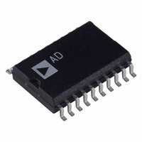
AD7703ARZ Analog Devices Inc, AD7703ARZ Datasheet - Page 6

AD7703ARZ
Manufacturer Part Number
AD7703ARZ
Description
IC ADC 20BIT LC2MOS 20-SOIC
Manufacturer
Analog Devices Inc
Datasheet
1.AD7703AR-REEL.pdf
(16 pages)
Specifications of AD7703ARZ
Data Interface
Serial
Number Of Bits
20
Sampling Rate (per Second)
4k
Number Of Converters
1
Power Dissipation (max)
37mW
Voltage Supply Source
Analog and Digital, Dual ±
Operating Temperature
-40°C ~ 85°C
Mounting Type
Surface Mount
Package / Case
20-SOIC (0.300", 7.50mm Width)
Resolution (bits)
20bit
Sampling Rate
4kSPS
Input Channel Type
Single Ended
Supply Voltage Range - Analog
± 4.5V To ± 5.5V
Supply Current
2.7mA
Number Of Elements
1
Resolution
20Bit
Architecture
Delta-Sigma
Sample Rate
16KSPS
Input Polarity
Unipolar/Bipolar
Input Type
Voltage
Rated Input Volt
2.5/±2.5V
Differential Input
No
Power Supply Requirement
Dual
Single Supply Voltage (typ)
Not RequiredV
Single Supply Voltage (min)
Not RequiredV
Single Supply Voltage (max)
Not RequiredV
Dual Supply Voltage (typ)
±5V
Dual Supply Voltage (min)
±4.5V
Dual Supply Voltage (max)
±5.5V
Power Dissipation
37mW
Differential Linearity Error
±0.5LSB(Typ)
Integral Nonlinearity Error
±0.003%FSR
Operating Temp Range
-40C to 85C
Operating Temperature Classification
Industrial
Mounting
Surface Mount
Pin Count
20
Package Type
SOIC W
Input Signal Type
Single-Ended
Package
20SOIC W
Number Of Analog Inputs
1
Digital Interface Type
Serial (SPI)
Polarity Of Input Voltage
Unipolar|Bipolar
Lead Free Status / RoHS Status
Lead free / RoHS Compliant
Lead Free Status / RoHS Status
Lead free / RoHS Compliant, Lead free / RoHS Compliant
Available stocks
Company
Part Number
Manufacturer
Quantity
Price
Part Number:
AD7703ARZ
Manufacturer:
ADI/亚德诺
Quantity:
20 000
AD7703
Pin No. Mnemonic Description
1
2
3
4, 17
5
6
7
8
9
10
11
12
13
14
15
16
18
19
20
MODE
CLKOUT
CLKIN
SC1, SC2
DGND
DV
AV
AGND
A
V
SLEEP
BP/UP
CAL
AV
DV
CS
DRDY
SCLK
SDATA
IN
REF
SS
DD
SS
DD
CLKOUT
CLKIN
MODE
DGND
AGND
PIN CONFIGURATION
DV
AV
V
SC1
DIP, CERDIP, SOIC
REF
A
SS
SS
IN
10
Selects the Serial Interface Mode. If MODE is tied to DGND, the Synchronous External Clocking (SEC)
mode is selected. SCLK is configured as an input, and the output appears without formatting, the MSB
coming first. If MODE is tied to +5 V, the AD7703 operates in the Synchronous Self-Clocking (SSC) mode.
SCLK is configured as an output, with a clock frequency for f
Clock Output to Generate an Internal Master Clock by Connecting a Crystal between CLKOUT and CLKIN.
If an external clock is used, CLKOUT is not connected.
Clock Input for External Clock.
System Calibration Pins. The state of these pins, when CAL is taken high, determines the type of calibration
performed.
Digital Ground. Ground reference for all digital signals.
Digital Negative Supply, –5 V Nominal.
Analog Negative Supply, –5 V Nominal.
Analog Ground. Ground reference for all analog signals.
Analog Input.
Voltage Reference Input, 2.5 V Nominal. This determines the value of positive full scale in the Unipolar
mode and the value of both positive and negative full scale in the Bipolar mode.
Sleep Mode Pin. When this pin is taken low, the AD7703 goes into a low power mode with typically 10 µW
power consumption.
Bipolar/Unipolar Mode Pin. When this pin is low, the AD7703 is configured for a unipolar input range going
from AGND to V
Calibration Mode Pin. When CAL is taken high for more than four cycles, the AD7703 is reset and performs
a calibration cycle when CAL is brought low again. The CAL pin can also be used as a strobe to synchronize
the operation of several AD7703s.
Analog Positive Supply, 5 V Nominal.
Digital Positive Supply, 5 V Nominal.
Chip Select Input. When CS is brought low, the AD7703 will begin to transmit serial data in a format determined
by the state of the MODE pin.
Data Ready Output. DRDY is low when valid data is available in the output register. It goes high after trans-
mission of a word is completed. It also goes high for four clock cycles when a new data-word is being loaded
into the output register, to indicate that valid data is not available, irrespective of whether data transmission
is complete or not.
Serial Clock Input/Output. The SCLK pin is configured as an input or output, dependent on the type of
serial data transmission that has been selected by the MODE pin. When configured as an output in the
Synchronous Self-Clocking mode, it has a frequency of f
Serial Data Output. The AD7703’s output data is available at this pin as a 20-bit serial word.
1
2
3
4
5
6
7
8
9
(Not to Scale)
TOP VIEW
AD7703
20
19
18
17
16
15
14
13
12
11
SDATA
SCLK
DRDY
CS
DV
AV
CAL
BP/UP
SLEEP
SC2
REF
DD
DD
. When Pin 12 is high, the AD7703 is configured for a bipolar input range, ±V
PIN FUNCTION DESCRIPTIONS
–6–
0.596 0.25
1.192 0.5
2.384 1.00
4.768 2.00
9.537 4.00
V
Table I. Bit Weight Table (2.5 V Reference Voltage)
LSB
CLKIN
Unipolar Mode
% FS
0.0000238
0.0000477
0.0000954
0.0001907
0.0003814
CLKIN
/4 and a duty cycle of 25%.
/4 and 25% duty cycle.
ppm
FS
0.24
0.48
0.95
1.91
3.81
LSB
0.13
0.26
0.5
1.00
2.00
Bipolar Mode
% FS
0.0000119 0.12
0.0000238 0.24
0.0000477 0.48
0.0000954 0.95
0.0001907 1.91
REF
REV. E
.
ppm
FS


