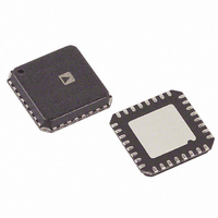
AD7266BCP Analog Devices Inc, AD7266BCP Datasheet - Page 19

AD7266BCP
Manufacturer Part Number
AD7266BCP
Description
IC ADC 12BIT 3CHAN 2MSPS 32LFCSP
Manufacturer
Analog Devices Inc
Datasheet
1.AD7266BCPZ-REEL.pdf
(28 pages)
Specifications of AD7266BCP
Design Resources
AD7266 SAR ADC in DC-Coupled Differential and Single-Ended Appls (CN0039)
Number Of Bits
12
Sampling Rate (per Second)
2M
Data Interface
DSP, MICROWIRE™, QSPI™, Serial, SPI™
Number Of Converters
2
Power Dissipation (max)
33.6mW
Voltage Supply Source
Analog and Digital
Operating Temperature
-40°C ~ 125°C
Mounting Type
Surface Mount
Package / Case
32-VFQFN, CSP Exposed Pad
For Use With
EVAL-AD7266CBZ - BOARD EVALUATION FOR AD7266
Lead Free Status / RoHS Status
Contains lead / RoHS non-compliant
MODES OF OPERATION
The mode of operation of the AD7266 is selected by controlling
the (logic) state of the
three possible modes of operation: normal mode, partial power-
down mode, and full power-down mode. After a conversion is
initiated, the point at which
power-down mode, if any, the device enters. Similarly, if already
in a power-down mode, CS can control whether the device
returns to normal operation or remains in power-down. These
modes of operation are designed to provide flexible power
management options. These options can be chosen to optimize
the power dissipation/throughput rate ratio for differing
application requirements.
NORMAL MODE
This mode is intended for applications needing fastest throughput
rates because the user does not have to worry about any power-
up times with the AD7266 remaining fully powered at all times.
Figure 34 shows the general diagram of the operation of the
AD7266 in this mode.
The conversion is initiated on the falling edge of CS , as
described in the Serial Interface section. To ensure that the part
remains fully powered up at all times, CS must remain low until
at least 10 SCLK falling edges have elapsed after the falling edge
of CS . If CS is brought high any time after the 10
edge but before the 14
powered up, but the conversion is terminated and D
D
required to complete the conversion and access the conversion
result. The D
SCLK cycles have elapsed, but instead does so when CS is
brought high again. If CS is left low for another 2 SCLK cycles
(for example, if only a 16 SCLK burst is available), two trailing
zeros are clocked out after the data. If CS is left low for a further
14 (or16) SCLK cycles, the result from the other ADC on board
is also accessed on the same D
(see the Serial Interface section).
Once 32 SCLK cycles have elapsed, the D
three-state on the 32
prior to this, the D
Therefore, CS may idle low after 32 SCLK cycles until it is
brought high again sometime prior to the next conversion
(effectively idling CS low), if so desired, because the bus still
returns to three-state upon completion of the dual result read.
D
D
SCLK
OUT
OUT
OUT
CS
A
B
B go back into three-state. Fourteen serial clock cycles are
OUT
1
line does not return to three-state after 14
LEADING ZEROS + CONVERSION RESULT
Figure 34. Normal Mode Operation
OUT
nd
th
CS signal during a conversion. There are
line returns to three-state at that point.
SCLK falling edge. If CS is brought high
SCLK falling edge, the part remains
CS is pulled high determines which
OUT
line, as shown in Figure 42
10
OUT
line returns to
th
14
SCLK falling
OUT
A and
Rev. A | Page 19 of 28
Once a data transfer is complete and D
returned to three-state, another conversion can be initiated after
the quiet time, t
(assuming the required acquisition time is allowed).
PARTIAL POWER-DOWN MODE
This mode is intended for use in applications where slower
throughput rates are required. Either the ADC is powered down
between each conversion, or a series of conversions may be
performed at a high throughput rate, and the ADC is then
powered down for a relatively long duration between these
bursts of several conversions. When the AD7266 is in partial
power-down, all analog circuitry is powered down except for
the on-chip reference and reference buffer.
To enter partial power-down mode, the conversion process
must be interrupted by bringing CS high anywhere after the
second falling edge of SCLK and before the 10
SCLK, as shown in
window of SCLKs, the part enters partial power-down, the
conversion that was initiated by the falling edge of CS is
terminated, and D
CS is brought high before the second SCLK falling edge, the
part remains in normal mode and does not power down. This
avoids accidental power-down due to glitches on the CS line.
To exit this mode of operation and power up the AD7266 again,
a dummy conversion is performed. On the falling edge of CS ,
the device begins to power up and continues to power up as
long as CS is held low until after the falling edge of the 10
SCLK. The device is fully powered up after approximately 1 μs
has elapsed, and valid data results from the next conversion, as
shown in Figure 36. If CS is brought high before the second
falling edge of SCLK, the AD7266 again goes into partial
power-down. This avoids accidental power-up due to glitches
on the CS line. Although the device may begin to power up on
the falling edge of CS , it powers down again on the rising edge
of CS . If the AD7266 is already in partial power-down mode
and CS is brought high between the second and 10
edges of SCLK, the device enters full power-down mode.
D
D
SCLK
OUT
OUT
CS
A
B
Figure 35. Entering Partial Power-Down Mode
QUIET
1
OUT
2
Figure 35. Once
, has elapsed by bringing
A and D
OUT
B go back into three-state. If
CS
OUT
is brought high in this
10
THREE-STATE
A and D
CS
th
falling edge of
low again
OUT
1
th
4
AD7266
falling
B have
th


