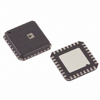
AD7266BCP Analog Devices Inc, AD7266BCP Datasheet - Page 3

AD7266BCP
Manufacturer Part Number
AD7266BCP
Description
IC ADC 12BIT 3CHAN 2MSPS 32LFCSP
Manufacturer
Analog Devices Inc
Datasheet
1.AD7266BCPZ-REEL.pdf
(28 pages)
Specifications of AD7266BCP
Design Resources
AD7266 SAR ADC in DC-Coupled Differential and Single-Ended Appls (CN0039)
Number Of Bits
12
Sampling Rate (per Second)
2M
Data Interface
DSP, MICROWIRE™, QSPI™, Serial, SPI™
Number Of Converters
2
Power Dissipation (max)
33.6mW
Voltage Supply Source
Analog and Digital
Operating Temperature
-40°C ~ 125°C
Mounting Type
Surface Mount
Package / Case
32-VFQFN, CSP Exposed Pad
For Use With
EVAL-AD7266CBZ - BOARD EVALUATION FOR AD7266
Lead Free Status / RoHS Status
Contains lead / RoHS non-compliant
SPECIFICATIONS
T
f
unless otherwise noted
Table 1.
Parameter
DYNAMIC PERFORMANCE
SAMPLE AND HOLD
DC ACCURACY
ANALOG INPUT
SCLK
A
Signal-to-Noise Ratio (SNR)
Signal-to-Noise + Distortion Ratio (SINAD)
Total Harmonic Distortion (THD)
Spurious-Free Dynamic Range (SFDR)
Intermodulation Distortion (IMD)
Channel-to-Channel Isolation
Aperture Delay
Aperture Jitter
Aperture Delay Matching
Full Power Bandwidth
Resolution
Integral Nonlinearity
Differential Nonlinearity
Straight Binary Output Coding
Twos Complement Output Coding
Single-Ended Input Range
Pseudo Differential Input Range: V
Fully Differential Input Range: V
= T
= 32 MHz, f
Second-Order Terms
Third-Order Terms
Offset Error
Offset Error Match
Gain Error
Gain Error Match
Positive Gain Error
Positive Gain Error Match
Zero Code Error
Zero Code Error Match
Negative Gain Error
Negative Gain Error Match
MIN
to T
MAX
T
5
S
3
, V
3
= 2 MSPS, V
DD
2
= 2.7 V to 3.6 V, f
1
.
2, 4
3
2
DRIVE
V
IN+
IN+
2
2
= 2.7 V to 5.25 V; specifications apply using internal reference or external reference = 2.5 V ± 1%,
IN+
and V
and V
− V
2
SCLK
IN−
IN−
IN−
2
6
= 24 MHz, f
Specification
71
69
70
68
–77
–73
–75
–88
–88
–88
11
50
200
3.5/3
12
±1
±1.5
±0.99
−0.99/+1.5
±7
±2
±2.5
±0.5
±2
±0.5
±5
±1
±2
±0.5
0 V to V
0 V to 2 × V
0 to V
2 × V
V
V
33/26
CM
CM
± V
± V
REF
REF
REF
REF
REF
S
= 1.5 MSPS, V
/2
REF
Rev. A | Page 3 of 28
Unit
dB min
dB min
dB min
dB min
dB max
dB max
dB max
dB typ
dB typ
dB typ
ns max
ps typ
ps max
MHz typ
MHz typ
Bits
LSB max
LSB max
LSB max
LSB max
LSB max
LSB typ
LSB max
LSB typ
LSB max
LSB typ
LSB max
LSB typ
LSB max
LSB typ
V
V
V
V
V
DRIVE
= 2.7 V to 3.6 V; V
Test Conditions/Comments
f
f
pseudo differential modes
f
f
pseudo differential modes
f
f
pseudo differential modes
f
fa = 30 kHz, fb = 50 kHz
@ 0.1 dB, V
±0.5 LSB typ; differential mode
±0.5 LSB typ; single-ended and pseudo
differential modes
Differential mode
Single-ended and pseudo differential modes
±2 LSB typ
RANGE pin low
RANGE pin high
RANGE pin low
RANGE pin high
V
V
@ 3 dB, V
IN
IN
IN
IN
IN
IN
IN
CM
CM
= 50 kHz sine wave; differential mode
= 50 kHz sine wave; single-ended and
= 50 kHz sine wave; differential mode
= 50 kHz sine wave; single-ended and
= 50 kHz sine wave; differential mode
= 50 kHz sine wave; single-ended and
= 50 kHz sine wave
= common-mode voltage
= V
REF
DD
DD
DD
= 5 V/V
= 4.75 V to 5.25 V,
= 5 V/V
DD
DD
= 3 V
= 3 V
7
= V
REF
/2
AD7266


