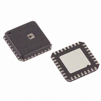
AD7266BCP Analog Devices Inc, AD7266BCP Datasheet - Page 4

AD7266BCP
Manufacturer Part Number
AD7266BCP
Description
IC ADC 12BIT 3CHAN 2MSPS 32LFCSP
Manufacturer
Analog Devices Inc
Datasheet
1.AD7266BCPZ-REEL.pdf
(28 pages)
Specifications of AD7266BCP
Design Resources
AD7266 SAR ADC in DC-Coupled Differential and Single-Ended Appls (CN0039)
Number Of Bits
12
Sampling Rate (per Second)
2M
Data Interface
DSP, MICROWIRE™, QSPI™, Serial, SPI™
Number Of Converters
2
Power Dissipation (max)
33.6mW
Voltage Supply Source
Analog and Digital
Operating Temperature
-40°C ~ 125°C
Mounting Type
Surface Mount
Package / Case
32-VFQFN, CSP Exposed Pad
For Use With
EVAL-AD7266CBZ - BOARD EVALUATION FOR AD7266
Lead Free Status / RoHS Status
Contains lead / RoHS non-compliant
AD7266
Parameter
REFERENCE INPUT/OUTPUT
LOGIC INPUTS
LOGIC OUTPUTS
CONVERSION RATE
POWER REQUIREMENTS
1
2
3
4
5
6
7
8
Temperature range is −40°C to +125°C.
See Terminology section.
Sample tested during initial release to ensure compliance.
Guaranteed no missed codes to 12 bits.
V
V
For full common-mode range, see Figure 24 and Figure 25.
Relates to Pin D
IN−
IN−
DC Leakage Current
Input Capacitance
Reference Output Voltage
Long-Term Stability
Output Voltage Hysteresis
Reference Input Voltage Range
DC Leakage Current
Input Capacitance
D
Reference Temperature Coefficient
V
Input High Voltage, V
Input Low Voltage, V
Input Current, I
Input Capacitance, C
Output High Voltage, V
Output Low Voltage, V
Floating State Leakage Current
Floating State Output Capacitance
Output Coding
Conversion Time
Track-and-Hold Acquisition Time
Throughput Rate
V
V
I
Power Dissipation
DD
REF
DD
DRIVE
CAP
or V
= 0 V for specified performance. For full input range on V
Normal Mode (Static)
Operational, f
Partial Power-Down Mode
Full Power-Down Mode (V
Normal Mode (Operational)
Partial Power-Down (Static)
Full Power-Down (Static)
A, D
Noise
IN+
must remain within GND/V
CAP
B Output Impedance
CAP
A or Pin D
IN
f
S
S
= 2 MSPS
= 1.5 MSPS
INL
IN
INH
3
CAP
OL
OH
B.
8
2
DD
DD
)
.
3
3
Specification
±1
45
10
2.5
150
50
0.1/V
±2
25
10
20
10
20
2.8
0.4
±15
5
V
0.4
±1
7
14
90
110
2
2.7/5.25
2.7/5.25
2.3
6.4
4
500
1
2.8
33.6
2.625
5.25
DRIVE
IN−
pin, see Figure 28 and Figure 29.
DD
− 0.2
Straight (natural) binary
Twos complement
Rev. A | Page 4 of 28
SCLK cycles
ns max
ns max
MSPS max
V min/V max
V min/V max
mA max
mA max
mA max
μA max
μA max
μA max
mW max
mW max
μW max
Unit
μA max
pF typ
pF typ
V min/V max
ppm typ
ppm typ
V min/V max
μA max
pF typ
Ω typ
ppm/°C max
ppm/°C typ
μV rms typ
V min
V max
nA typ
pF typ
V min
V max
μA max
pF typ
Test Conditions/Comments
When in track
When in hold
±0.2% max @ 25°C
For 1000 hours
See Typical Performance Characteristics section
External reference applied to Pin D
V
SGL/DIFF = 1 with 0 V to V
SGL/DIFF = 0; SGL/DIFF = 1 with 0 V to 2 × V
437.5 ns with SCLK = 32 MHz
Full-scale step input; V
Full-scale step input; V
Digital I/Ps = 0 V or V
V
V
V
Static
T
T
V
V
V
A
A
IN
DD
DD
DD
DD
DD
DD
= −40°C to +85°C
> 85°C to 125°C
= 0 V or V
= 5.25 V
= 5.25 V; 5.7 mA typ
= 3.6 V; 3.4 mA typ
= 5.25 V
= 5.25 V
= 5.25 V, T
DRIVE
A
= −40°C to +85°C
DRIVE
DD
DD
= 5 V
= 3 V
REF
range selected
CAP
A/Pin D
REF
range
CAP
B


