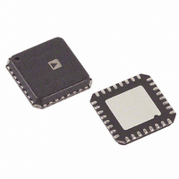
AD7266BCP Analog Devices Inc, AD7266BCP Datasheet - Page 8

AD7266BCP
Manufacturer Part Number
AD7266BCP
Description
IC ADC 12BIT 3CHAN 2MSPS 32LFCSP
Manufacturer
Analog Devices Inc
Datasheet
1.AD7266BCPZ-REEL.pdf
(28 pages)
Specifications of AD7266BCP
Design Resources
AD7266 SAR ADC in DC-Coupled Differential and Single-Ended Appls (CN0039)
Number Of Bits
12
Sampling Rate (per Second)
2M
Data Interface
DSP, MICROWIRE™, QSPI™, Serial, SPI™
Number Of Converters
2
Power Dissipation (max)
33.6mW
Voltage Supply Source
Analog and Digital
Operating Temperature
-40°C ~ 125°C
Mounting Type
Surface Mount
Package / Case
32-VFQFN, CSP Exposed Pad
For Use With
EVAL-AD7266CBZ - BOARD EVALUATION FOR AD7266
Lead Free Status / RoHS Status
Contains lead / RoHS non-compliant
AD7266
Pin No.
28, 30
31
32
Mnemonic
D
D
V
DV
DRIVE
OUT
OUT
DD
A,
B
Description
Serial Data Outputs. The data output is supplied to each pin as a serial data stream. The bits are clocked out on the
falling edge of the SCLK input and 14 SCLKs are required to access the data. The data simultaneously appears on
both pins from the simultaneous conversions of both ADCs. The data stream consists of two leading zeros
followed by the 12 bits of conversion data. The data is provided MSB first. If CS is held low for 16 SCLK cycles rather
than 14, then two trailing zeros will appear after the 12 bits of data. If CS is held low for a further 16 SCLK cycles on
either D
conversion on both ADCs to be gathered in serial format on either D
the Serial Interface section.
Logic Power Supply Input. The voltage supplied at this pin determines at what voltage the interface operates. This
pin should be decoupled to DGND. The voltage at this pin may be different than that at AV
never exceed either by more than 0.3 V.
Digital Supply Voltage, 2.7 V to 5.25 V. This is the supply voltage for all digital circuitry on the AD7266. The DV
and AV
transient basis. This supply should be decoupled to DGND.
DD
OUT
voltages should ideally be at the same potential and must not be more than 0.3 V apart even on a
A or D
OUT
B, the data from the other ADC follows on the D
Rev. A | Page 8 of 28
OUT
OUT
pin. This allows data from a simultaneous
A or D
OUT
B using only one serial port. See
DD
and DV
DD
but should
DD


