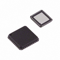
AD9717BCPZ Analog Devices Inc, AD9717BCPZ Datasheet - Page 40

AD9717BCPZ
Manufacturer Part Number
AD9717BCPZ
Description
IC DAC DUAL 14BIT LO PWR 40LFCSP
Manufacturer
Analog Devices Inc
Series
TxDAC®r
Datasheet
1.AD9717BCPZ.pdf
(80 pages)
Specifications of AD9717BCPZ
Data Interface
Serial
Number Of Bits
14
Number Of Converters
2
Voltage Supply Source
Analog and Digital
Power Dissipation (max)
86mW
Operating Temperature
-40°C ~ 85°C
Mounting Type
Surface Mount
Package / Case
40-LFCSP
Resolution (bits)
14bit
Sampling Rate
125MSPS
Input Channel Type
Parallel, Serial
Supply Current
11mA
Digital Ic Case Style
CSP
No. Of Pins
40
Lead Free Status / RoHS Status
Lead free / RoHS Compliant
Settling Time
-
Lead Free Status / RoHS Status
Lead free / RoHS Compliant, Lead free / RoHS Compliant
Available stocks
Company
Part Number
Manufacturer
Quantity
Price
Company:
Part Number:
AD9717BCPZ
Manufacturer:
ADI
Quantity:
172
Part Number:
AD9717BCPZ
Manufacturer:
ADI/亚德诺
Quantity:
20 000
AD9714/AD9715/AD9716/AD9717
DIGITAL INTERFACE OPERATION
Digital data for the I and Q DACs is supplied over a single
parallel bus (DB[n:0), where n is 7 for the AD9714, 9 for
the AD9715, 11 for the AD9716, and 13 for the AD9717)
accompanied by a qualifying clock (DCLKIO). The I and Q
data are provided to the chip in an interleaved double data
rate (DDR) format. The maximum guaranteed data rate is
250 MSPS with a 125 MHz clock. The order of data pairing
and the sampling edge selection is user programmable using
the IFIRST and IRISING data control bits, resulting in four
possible timing diagrams. These are shown in Figure 89,
NOTES:
1. DB[n:0], WHERE n IS 7 FOR THE AD9714, 9 FOR THE AD9715, 11 FOR THE
NOTES:
1. DB[n:0], WHERE n IS 7 FOR THE AD9714, 9 FOR THE AD9715, 11 FOR THE
DCLKIO
Q DATA
DCLKIO
Q DATA
DB[n:0]
DB[n:0]
I DATA
I DATA
AD9716, AND 13 FOR THE AD9717.
AD9716, AND 13 FOR THE AD9717.
90, Figure 91, and Figure 92.
Z
Z
Figure 89. Timing Diagram with IFIRST = 0, IRISING = 0
Figure 90. Timing Diagram with IFIRST = 0, IRISING = 1
A
A
B
B
Y
X
Z
Y
C
C
D
D
B
A
A
Z
E
E
F
F
D
C
C
B
G
G
H
H
D
E
E
F
Rev. A | Page 40 of 80
Ideally, the rising and falling edges of the clock fall in the center
of the keep-in-window formed by the setup and hold times, t
and t
timing diagram is shown in Figure 93.
In addition to the different timing modes listed in Table 2, the
input data can also be presented to the device in either unsigned
binary or twos complement format. The format type is chosen
via the TWOS data control bit.
DCLKIO
Q DATA
NOTES:
1. DB[n:0], WHERE n IS 7 FOR THE AD9714, 9 FOR THE AD9715, 11 FOR THE
NOTES:
1. DB[n:0], WHERE n IS 7 FOR THE AD9714, 9 FOR THE AD9715, 11 FOR THE
DCLKIO
Q DATA
DB[n:0]
DB[n:0]
I DATA
I DATA
AD9716, AND 13 FOR THE AD9717.
AD9716, AND 13 FOR THE AD9717.
H
. Refer to Table 2 for setup and hold times. A detailed
Z
Z
DCLKIO
NOTES:
1. DB[n:0], WHERE n IS 7 FOR THE AD9714, 9 FOR THE
DB[n:0]
Figure 91. Timing Diagram with IFIRST = 1, IRISING = 0
Figure 92. Timing Diagram with IFIRST = 1, IRISING = 1
Figure 93. Setup and Hold Times for All Input Modes
AD9715, 11 FOR THE AD9716, AND 13 FOR THE AD9717.
A
A
B
B
A
Z
Y
Z
t
S
t
C
C
H
D
D
B
C
B
A
t
S
t
H
E
E
F
F
D
C
D
E
G
G
H
H
G
E
F
F
S


