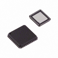
AD9717BCPZ Analog Devices Inc, AD9717BCPZ Datasheet - Page 41

AD9717BCPZ
Manufacturer Part Number
AD9717BCPZ
Description
IC DAC DUAL 14BIT LO PWR 40LFCSP
Manufacturer
Analog Devices Inc
Series
TxDAC®r
Datasheet
1.AD9717BCPZ.pdf
(80 pages)
Specifications of AD9717BCPZ
Data Interface
Serial
Number Of Bits
14
Number Of Converters
2
Voltage Supply Source
Analog and Digital
Power Dissipation (max)
86mW
Operating Temperature
-40°C ~ 85°C
Mounting Type
Surface Mount
Package / Case
40-LFCSP
Resolution (bits)
14bit
Sampling Rate
125MSPS
Input Channel Type
Parallel, Serial
Supply Current
11mA
Digital Ic Case Style
CSP
No. Of Pins
40
Lead Free Status / RoHS Status
Lead free / RoHS Compliant
Settling Time
-
Lead Free Status / RoHS Status
Lead free / RoHS Compliant, Lead free / RoHS Compliant
Available stocks
Company
Part Number
Manufacturer
Quantity
Price
Company:
Part Number:
AD9717BCPZ
Manufacturer:
ADI
Quantity:
172
Part Number:
AD9717BCPZ
Manufacturer:
ADI/亚德诺
Quantity:
20 000
DIGITAL DATA LATCHING AND RETIMER BLOCK
The AD9714/AD9715/AD9716/AD9717 have two clock inputs,
DCLKIO and CLKIN. The CLKIN is the analog clock whose
jitter affects DAC performance, and the DCLKIO is a digital
clock from an FPGA that needs to have a fixed relationship with
the input data to ensure that the data is picked
up correctly by the flip-flops on the pads.
Figure 94 is a simplified diagram of the entire data capture
system in the AD9714/AD9715/AD9716/AD9717. The double
data rate input data (DB[n:0), where n is 7 for the AD9714, 9
for the AD9715, 11 for the AD9716, and 13 for the AD9717) is
latched at the pads/pins either on the rising edge or the falling edge
of the DCLKIO-INT clock, as determined by IRISING, Bit 4 of
SPI Address 0x02. Bit 5 of SPI Address 0x02, IFIRST, determines
which channel data is latched first (that is, I or Q). The captured
data is then retimed to the internal clock (CLKIN-INT) in the
retimer block before being sent to the final analog DAC core
(D-FF 4), which controls the current steering output switches. All
delay blocks depicted in Figure 94 are noninverting, and any wires
without an explicit delay block can be assumed to have no delay.
Only one channel is shown in Figure 94 with the data pads
(DB[n:0), where n is 7 for the AD9714, 9 for the AD9715, 11 for
the AD9716, and 13 for the AD9717) serving as double data
rate pads for both channels.
The default PINMD and SPI settings are IE = high (closed)
and OE = low (open). These settings are enabled when RESET/
PINMD (Pin 35) is held high. In this mode, the user has to supply
both DCLKIO and CLKIN. In PINMD, it is also recommended
that the DCLKIO and the CLKIN be in phase for proper func-
tioning of the DAC, which can easily be ensured by tying the
pins together on the PCB. If the user can access the SPI, setting
Bit 2 of SPI Address 0x02, DCI_EN, to logic low causes the
CLKIN to be used as the DCLKIO also.
NOTES:
1. DB[n:0], WHERE n IS 7 FOR THE AD9714, 9 FOR THE AD9715, 11 FOR THE AD9716, AND 13 FOR THE AD9717.
DB[n:0]
(INPUT)
D-FF
OR
0
Figure 94. Simplified Diagram of AD9714/AD9715/AD9716/AD9717 Timing
DCLKIO-INT
(INPUT/OUTPUT)
IE
DCLKIO
D-FF
1
Rev. A | Page 41 of 80
DELAY2
IE
D-FF
2
RETIMER-CLK
Setting Bit 1 or Bit 0 of SPI Address 0x02, DCOSGL or DCODBL,
respectively, to logic high allows the user to obtain a DCLKIO
output from the CLKIN input for use in the user’s PCB system.
It is strongly recommended that DCI_EN = DCOSGL = high or
DCI_EN = DCODBL = high not be used even though the
device may appear to function correctly. Similarly, do not set
DCOSGL and DCODBL to logic high simultaneously.
Retimer
The AD9714/AD9715/AD9716/AD9717 have an internal data
retimer circuit that compares the CLKIN-INT and DCLKIO-INT
clocks and, depending on their phase relationship, selects a
retimer clock (RETIMER-CLK) to safely transfer data from
the DCLKIO used at the chip’s input interface to the CLKIN
used to clock the analog DAC cores (D-FF 4).
The retimer selects one of the three phases shown in Figure 95.
The retimer is controlled by the CLKMODE SPI bits, as shown
in Table 15.
Note that, in most cases, more than one retimer phase works
and ,in such cases, the retimer arbitrarily picks one phase that
works. The retimer cannot pick the best or safest phase. If the
user has a working knowledge of the exact phase relationship
between DCLKIO and CLKIN (and thus DCLKIO-INT and
CLKIN-INT because the delay is approximately the same for
both clocks and equal to DELAY1), then the retimer can be
forced to this phase with CLKMODEN = 1, as described in
Table 15 and the following paragraphs.
D-FF
OE
3
(INPUT)
CLKIN
NOTES
D-FFs:
0: RISING OR FALLING EDGE
TRIGGERED FOR I OR Q DATA.
1, 2, 3, 4: RISING EDGE TRIGGERED.
AD9714/AD9715/AD9716/AD9717
CLOCK
DATA
TO DAC CORE
CLKIN-INT
Figure 95. RETIMER-CLK Phases
1/2 PERIOD
1/4 PERIOD
D-FF
4
1/2 PERIOD
RETIMER-CLKs
I
OUT
I
OUT
180°
90°
270°


