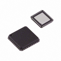
AD9717BCPZ Analog Devices Inc, AD9717BCPZ Datasheet - Page 49

AD9717BCPZ
Manufacturer Part Number
AD9717BCPZ
Description
IC DAC DUAL 14BIT LO PWR 40LFCSP
Manufacturer
Analog Devices Inc
Series
TxDAC®r
Datasheet
1.AD9717BCPZ.pdf
(80 pages)
Specifications of AD9717BCPZ
Data Interface
Serial
Number Of Bits
14
Number Of Converters
2
Voltage Supply Source
Analog and Digital
Power Dissipation (max)
86mW
Operating Temperature
-40°C ~ 85°C
Mounting Type
Surface Mount
Package / Case
40-LFCSP
Resolution (bits)
14bit
Sampling Rate
125MSPS
Input Channel Type
Parallel, Serial
Supply Current
11mA
Digital Ic Case Style
CSP
No. Of Pins
40
Lead Free Status / RoHS Status
Lead free / RoHS Compliant
Settling Time
-
Lead Free Status / RoHS Status
Lead free / RoHS Compliant, Lead free / RoHS Compliant
Available stocks
Company
Part Number
Manufacturer
Quantity
Price
Company:
Part Number:
AD9717BCPZ
Manufacturer:
ADI
Quantity:
172
Part Number:
AD9717BCPZ
Manufacturer:
ADI/亚德诺
Quantity:
20 000
DIFFERENTIAL BUFFERED OUTPUT
USING AN OP AMP
A dual op amp (see the circuit shown in Figure 105) can be used
in a differential version of the single-ended buffer shown in
Figure 104. The same RC network is used to form a one-pole
differential, low-pass filter to isolate the op amp inputs from
the high frequency images produced by the DAC outputs. The
feedback resistors, R
signal swing by the formula
The maximum and minimum single-ended voltages out of the
amplifier are, respectively,
The common-mode voltage of the differential output is
determined by the formula
AUXILIARY DACs
The DACs of the AD9714/AD9715/AD9716/AD9717 feature
two versatile and independent 10-bit auxiliary DACs suitable
for dc offset correction and similar tasks.
Because the AUXDACs are driven through the SPI port, they
should never be used in timing-critical applications, such
as inside analog feedback loops.
AD9714/AD9715/
AD9716/AD9717
V
V
V
V
OUT
MIN
CM
MAX
= V
= V
= 2 × R
V
MAX
MAX
Figure 105. Single-Supply Differential Buffer
IOUTN
IOUTP
REF
REFIO
AVSS
− R
FB
− R
× I
28
34
25
29
FB
FB
FB
1
, determine the differential peak-to-peak
FS
× I
× I
R
R
R
FS
FS
S
FB
B
R
S
C
R
R
B
B
ADA4841-2
ADA4841-2
–
+
+
–
R
R
C
C
FB
FB
F
F
V
OUT
Rev. A | Page 49 of 80
To keep the pin count reasonable, these auxiliary DACs each
share a pin with the corresponding FSADJx resistor. They are,
therefore, usable only when enabled and when that DAC is
operated on its internal full-scale resistors. A simple I-to-V
converter is implemented on chip with selectable shunt resistors
(3.2 kΩ to 16 kΩ) such that if REFIO is set to exactly 1 V, REFIO/2
equals 0.5 V and the following equation describes the no load
output voltage:
Figure 106 illustrates the function of all the SPI bits controlling
these DACs with the exception of the QAUXEN (Register 0x0A,
Bit 7) and IAUXEN (Register 0x0C, Bit 7) bits and gating to
prohibit R
The SPI speed limits the update rate of the auxiliary DACs. The
data is inverted such that I
at 0x1FF, as shown in Figure 107.
Figure 107. AUXDAC Op Amp Output vs. Current, AVDD = 3.3 V, No Load,
RNG0
RNG1
OFS2
OFS1
OFS0
V
OUT
3.0
2.8
2.6
2.4
2.2
2.0
1.8
1.6
1.4
1.2
1.0
0.8
0.6
0.4
0.2
0
AUXDAC
0
[9:0]
S
(OFS > 4 = 4)
4kΩ
AD9714/AD9715/AD9716/AD9717
< 3.2 kΩ.
10
Figure 106. AUXDAC Simplified Circuit Diagram
0
5 .
8kΩ
20
V
OP AMP OUTPUT VOLTAGE vs. CHANGES
IN R
30
16kΩ 16kΩ
OFFSET
I
AUXDAC 0x1FF to 0x000
DAC
40
AUXDAC
AVDD
AND DAC CURRENT IN µA
50
REFIO
I
1
AUXDAC
R
2
5 .
S
60
is full scale at 0x000 and zero
16
RNG: 00 = > 125µA
70
(µA)
k
–
+
OP AMP
80
01 = > 62µA
10 = > 31µA
11 = > 16µA
16kΩ
R
R
R
R
R
90
OFFSET
OFFSET
OFFSET
OFFSET
OFFSET
100
f
f
f
S
S
S
f
= 3.3kΩ
= 4kΩ
= 5.3kΩ
= 8kΩ
= 16kΩ
110
S
120 130
AUX
PIN


