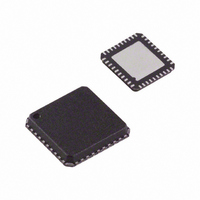
AD9717BCPZ Analog Devices Inc, AD9717BCPZ Datasheet - Page 51

AD9717BCPZ
Manufacturer Part Number
AD9717BCPZ
Description
IC DAC DUAL 14BIT LO PWR 40LFCSP
Manufacturer
Analog Devices Inc
Series
TxDAC®r
Datasheet
1.AD9717BCPZ.pdf
(80 pages)
Specifications of AD9717BCPZ
Data Interface
Serial
Number Of Bits
14
Number Of Converters
2
Voltage Supply Source
Analog and Digital
Power Dissipation (max)
86mW
Operating Temperature
-40°C ~ 85°C
Mounting Type
Surface Mount
Package / Case
40-LFCSP
Resolution (bits)
14bit
Sampling Rate
125MSPS
Input Channel Type
Parallel, Serial
Supply Current
11mA
Digital Ic Case Style
CSP
No. Of Pins
40
Lead Free Status / RoHS Status
Lead free / RoHS Compliant
Settling Time
-
Lead Free Status / RoHS Status
Lead free / RoHS Compliant, Lead free / RoHS Compliant
Available stocks
Company
Part Number
Manufacturer
Quantity
Price
Company:
Part Number:
AD9717BCPZ
Manufacturer:
ADI
Quantity:
172
Part Number:
AD9717BCPZ
Manufacturer:
ADI/亚德诺
Quantity:
20 000
Note that LO feedthrough compensation is independent of
phase compensation. However, gain compensation can affect
the LO compensation because the gain compensation may
change the common-mode level of the signal. The dc offset of
some modulators is common-mode level dependent. Therefore,
it is recommended that the gain adjustment be performed prior
to LO compensation.
LO FEEDTHROUGH COMPENSATION
To achieve LO feedthrough compensation in a circuit, each
output of the two AUXDACs must be connected through a
100 kΩ resistor to one side of the differential DAC output. See
the Auxiliary DACS section for details of how to use AUXDACs.
The purpose of these connections is to drive a very small amount
of current into the nodes at the quadrature modulator inputs,
thereby adding a slight dc bias to one or the other of the
quadrature modulator signal inputs.
To achieve LO feedthrough compensation, the user should start
with the default conditions of the AUXDAC registers, and then
increment the magnitude of one or the other AUXDAC output
voltages. While this is being done, the amplitude of the LO
feedthrough at the quadrature modulator output should be
sensed. If the LO feedthrough amplitude increases, try either
decreasing the output voltage of the AUXDAC being adjusted,
or try adjusting the output voltage of the other AUXDAC. It
may take practice before an effective algorithm is achieved. The
AD9714/AD9715/AD9716/AD9717 evaluation board can be
used to adjust the LO feedthrough down to the noise floor,
although this is not stable over temperature.
RESULTS OF GAIN AND OFFSET CORRECTION
The results of gain and offset correction can be seen in Figure 110
and Figure 111. Figure 110 shows the output spectrum of the
quadrature demodulator before gain and offset correction.
Figure 111 shows the output spectrum after correction. The
LO feedthrough spur at 450 MHz has been suppressed to the
noise level. This result can be achieved by applying the correc-
tion, but the correction must be repeated after a large change in
temperature.
Note that gain matching improves the negative frequency image
rejection, but it is also related to the phase mismatch in the
quadrature modulator. It can be improved by adjusting the
relative phase between the two quadrature signals at the digital
side or properly designing the low-pass filter between the DACs
and quadrature modulators. Phase mismatch is frequency depen-
dent; therefore, routines must be developed to adjust it if
wideband signals are desired.
Rev. A | Page 51 of 80
Figure 110. AD9714/AD9715/AD9716/AD9717 and ADL5370 with a Single-
Figure 111. AD9714/AD9715/AD9716/AD9717 and ADL5370 with a Single-
–10
–15
–20
–25
–30
–35
–40
–45
–50
–55
–60
–65
–70
–75
–80
–85
–90
–95
–10
–15
–20
–25
–30
–35
–40
–45
–50
–55
–60
–65
–70
–75
–80
–85
–90
–95
Tone Signal at 450 MHz, Gain and LO Compensation Optimized
–5
–5
447.5
447.5
5
0
5
0
Tone Signal at 450 MHz, No Gain or LO Compensation
AD9714/AD9715/AD9716/AD9717
449.0
449.0
FREQUENCY (MHz)
FREQUENCY (MHz)
450.0
450.0
451.0
451.0
452.5
452.5


