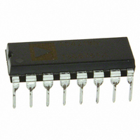
AD7243AN Analog Devices Inc, AD7243AN Datasheet - Page 10

AD7243AN
Manufacturer Part Number
AD7243AN
Description
IC SRL DAC 12BIT LC2MOS 16-DIP
Manufacturer
Analog Devices Inc
Series
DACPORT®r
Datasheet
1.AD7243ANZ.pdf
(12 pages)
Specifications of AD7243AN
Data Interface
Serial
Settling Time
10µs
Rohs Status
RoHS non-compliant
Number Of Bits
12
Number Of Converters
1
Voltage Supply Source
Dual ±
Power Dissipation (max)
100mW
Operating Temperature
-40°C ~ 85°C
Mounting Type
Through Hole
Package / Case
16-DIP (0.300", 7.62mm)
Resolution (bits)
12bit
Digital Ic Case Style
DIP
No. Of Pins
16
Operating Temperature Range
-40°C To +85°C
Update Rate
0.1MSPS
Package
16PDIP
Resolution
12 Bit
Conversion Rate
300 KSPS
Architecture
R-2R
Digital Interface Type
Serial (3-Wire)
Number Of Outputs Per Chip
1
Output Type
Voltage
Full Scale Error
±6 LSB
Integral Nonlinearity Error
±1 LSB
Maximum Settling Time
10 us
Number Of Channels
1
Interface Type
Serial (3-Wire)
Single Supply Voltage (typ)
12/15V
Dual Supply Voltage (typ)
±12/±15V
Power Supply Requirement
Single/Dual
Single Supply Voltage (min)
10.8V
Single Supply Voltage (max)
16.5V
Dual Supply Voltage (min)
±10.8V
Dual Supply Voltage (max)
±16.5V
Operating Temp Range
-40C to 85C
Operating Temperature Classification
Industrial
Mounting
Through Hole
Pin Count
16
Package Type
PDIP
Lead Free Status / Rohs Status
Not Compliant
Available stocks
Company
Part Number
Manufacturer
Quantity
Price
Company:
Part Number:
AD7243AN
Manufacturer:
AD
Quantity:
5 510
Company:
Part Number:
AD7243ANZ
Manufacturer:
AMTEL
Quantity:
648
Part Number:
AD7243ANZ
Manufacturer:
ADI/亚德诺
Quantity:
20 000
AD7243
AD7243–87C51 Interface
A serial interface between the AD7243 and the 87C51
microcontroller is shown in Figure 14. TXD of the 87C51 drives
SCLK of the AD7243, while RXD drives the serial data line of
the part. The SYNC signal is derived from the port line P3.3.
The 87C51 provides the LSB of its SBUF register as the first bit
in the serial data stream. Therefore, the user will have to ensure
that the data in the SBUF register is arranged correctly so that
the don’t care bits are the first to be transmitted to the AD7243
and the last bit to be sent is the LSB of the word to be loaded to
the AD7243. When data is to be transmitted to the part, P3.3 is
taken low. Data on RXD is valid on the falling edge of TXD.
The 87C51 transmits its serial data in 8-bit bytes with only eight
falling clock edges occurring in the transmit cycle. To load data
to the AD7243, P3.3 is left low after the first eight bits are trans-
ferred and a second byte of data is then transferred serially to the
AD7243. When the second serial transfer is complete, the P3.3
line is taken high.
Figure 14 shows the LDAC input of the AD7243 hard wired
low. As a result, the DAC latch and the analog output will be up-
dated on the sixteenth falling edge of TXD after the SYNC sig-
nal for the DAC has gone low. Alternatively, the scheme used in
previous interfaces, whereby the LDAC input is driven from a
timer, can be used.
AD7243–68HC11 Interface
Figure 15 shows a serial interface between the AD7243 and the
68HC11 microcontroller. SCK of the 68HC11 drives SCLK of
the AD7243 while the MOSI output drives the serial data line of
the AD7243. The SYNC signal is derived from a port line (PC7
shown).
For correct operation of this interface, the 68HC11 should be
configured such that its CPOL bit is a 0 and its CPHA bit is a 1.
When data is to be transmitted to the part, PC7 is taken low.
When the 68HC11 is configured like this, data on MOSI is valid
on the falling edge of SCK. The 68HC11 transmits its serial data
in 8-bit bytes with only eight falling clock edges occurring in the
transmit cycle. To load data to the AD7243, PC7 is left low after
the first eight bits are transferred and a second byte of data is
then transferred serially to the AD7243. When the second serial
transfer is complete, the PC7 line is taken high.
*ADDITIONAL PINS OMITTED FOR CLARITY
87C51*
P3.3
RXD
TXD
LDAC
SYNC
SCLK
SDIN
AD7243*
Figure 15 shows the LDAC input of the AD7243 hardwired
low. As a result, the DAC latch and the analog output of the
DAC will be updated on the sixteenth falling edge of SCK after
the respective SYNC signal has gone low. Alternatively, the
scheme used in previous interfaces, whereby the LDAC input is
driven from a timer, can be used.
Multiple DAC Daisy-Chain Interface
A multi-DAC serial interface is shown in Figure 16. This
scheme may be used with all of the interfaces previously dis-
cussed if more than one DAC is required in a system. To enable
the facility the DCEN pin must be connected high on all de-
vices, including the last device in the chain.
*ADDITIONAL PINS OMITTED FOR CLARITY
MICROCONTROLLER
*ADDITIONAL PINS OMITTED FOR CLARITY
68HC11*
MOSI
SCK
PC7
PA0
PA1
PA2
PA3
LDAC
SYNC
SCLK
SDIN
AD7243*
SCLK
SYNC
SCLK
SYNC
LDAC
LDAC
SCLK
SYNC
LDAC
AD7243*
AD7243*
AD7243*
SDO
SDO
SDIN
SDIN
SDO
SDIN
DCEN
DCEN
DCEN
V
V
V
DD
DD
DD


