AD7243AN Analog Devices Inc, AD7243AN Datasheet - Page 4
AD7243AN
Manufacturer Part Number
AD7243AN
Description
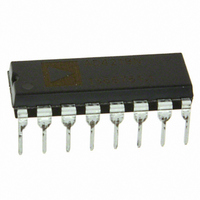
IC SRL DAC 12BIT LC2MOS 16-DIP
Manufacturer
Analog Devices Inc
Series
DACPORT®r
Datasheet
1.AD7243ANZ.pdf
(12 pages)
Specifications of AD7243AN
Data Interface
Serial
Settling Time
10µs
Rohs Status
RoHS non-compliant
Number Of Bits
12
Number Of Converters
1
Voltage Supply Source
Dual ±
Power Dissipation (max)
100mW
Operating Temperature
-40°C ~ 85°C
Mounting Type
Through Hole
Package / Case
16-DIP (0.300", 7.62mm)
Resolution (bits)
12bit
Digital Ic Case Style
DIP
No. Of Pins
16
Operating Temperature Range
-40°C To +85°C
Update Rate
0.1MSPS
Package
16PDIP
Resolution
12 Bit
Conversion Rate
300 KSPS
Architecture
R-2R
Digital Interface Type
Serial (3-Wire)
Number Of Outputs Per Chip
1
Output Type
Voltage
Full Scale Error
±6 LSB
Integral Nonlinearity Error
±1 LSB
Maximum Settling Time
10 us
Number Of Channels
1
Interface Type
Serial (3-Wire)
Single Supply Voltage (typ)
12/15V
Dual Supply Voltage (typ)
±12/±15V
Power Supply Requirement
Single/Dual
Single Supply Voltage (min)
10.8V
Single Supply Voltage (max)
16.5V
Dual Supply Voltage (min)
±10.8V
Dual Supply Voltage (max)
±16.5V
Operating Temp Range
-40C to 85C
Operating Temperature Classification
Industrial
Mounting
Through Hole
Pin Count
16
Package Type
PDIP
Lead Free Status / Rohs Status
Not Compliant
Available stocks
Company
Part Number
Manufacturer
Quantity
Price
Company:

Part Number:
AD7243AN
Manufacturer:
AD
Quantity:
5 510
Company:
Part Number:
AD7243ANZ
Manufacturer:
AMTEL
Quantity:
648
Part Number:
AD7243ANZ
Manufacturer:
ADI/亚德诺
Quantity:
20 000


AD7243
TERMINOLOGY
Bipolar Zero Error
Bipolar Zero Error is the voltage measured at V
DAC is configured for bipolar output and loaded with all 0s
(Two’s Complement Coding) or with 1000 0000 0000 (Offset
Binary Coding). It is due to a combination of offset errors in the
DAC, amplifier and mismatch between the internal gain resis-
tors around the amplifier.
Full-Scale Error
Full-Scale Error is a measure of the output error when the am-
plifier output is at full scale (for the bipolar output range full
scale is either positive or negative full scale). It is measured with
respect to the reference input voltage and includes the offset
errors.
Digital-to-Analog Glitch Impulse
This is the voltage spike that appears at V
code in the DAC latch changes, before the output settles to its
final value. The energy in the glitch is specified in nV secs, and
is measured for an all codes change from 0000 0000 0000 to
1111 1111 1111 and vice versa.
Digital Feedthrough
This is a measure of the voltage spike that appears on V
result of feedthrough from the digital inputs on the AD7243. It
is measured with LDAC held high.
Pin Mnemonic
1
2
3
4
5
6
7
8
9
10
11
12
13
14
15
16
REFIN
REFOUT
CLR
BIN/COMP
SCLK
SDIN
SYNC
DGND
LDAC
DCEN
SDO
AGND
R
V
V
V
OFS
OUT
SS
DD
Description
Voltage Reference Input. It is internally buffered before being applied to the DAC. The nominal reference
voltage for specified operation of the AD7243 is 5 V.
Voltage Reference Output. The internal 5 V analog reference is provided at this pin. To operate the part -
using its internal reference, REFOUT should be connected to REFIN.
Clear, Logic Input. Taking this input low sets V
bipolar range and to –REFIN in the offset binary bipolar range.
Logic Input. This input selects the data format to be either binary or two’s complement. In both unipolar
ranges, natural binary format is selected by connecting this input to a Logic “0.” In the bipolar configuration,
offset binary format is selected with a Logic “0” while a Logic “1” selects two’s complement format.
Serial Clock, Logic Input. Data is clocked into the input register on each falling SCLK edge.
Serial Data In, Logic Input. The 16-bit serial data word is applied to this input.
Data Synchronization Pulse, Logic Input. Taking this input low initializes the internal logic in readiness for a
new data word.
Digital Ground. Ground reference for all digital circuitry.
Load DAC, Logic Input. Updates the DAC output. The DAC output is updated on the falling edge of this
signal or alternatively if this line is permanently low, an automatic update mode is selected whereby the DAC
is updated on the 16th falling SCLK pulse.
Daisy-Chain Enable, Logic Input. Connect this pin high if a daisy-chain interface is being used, otherwise
this pin must be connected low.
Serial Data Out, Logic Output. With DCEN at Logic “1” this output is enabled, and the serial data in the
input shift register is clocked out on each falling SCLK edge.
Analog Ground. Ground reference for all analog circuitry.
Output Offset Resistor for the amplifier. It is connected to V
range and to REFIN for the –5 V to +5 V range.
Analog Output Voltage. This is the buffer amplifier output voltage. Three different output voltage ranges can
be chosen: 0 V to +5 V, 0 to +10 V and –5 V to +5 V.
Negative Power Supply (used for the output amplifier only, may be connected to 0 V for single supply
operation or to –12 V to –15 V for dual supplies).
Positive Power Supply (+12 V to +15 V).
AD7243 PIN FUNCTION DESCRIPTIONS (DIP and SOIC PIN NUMBERS)
OUT
when the digital
OUT
when the
OUT
as a
Relative Accuracy (Linearity)
Relative Accuracy, or endpoint linearity, is a measure of the
maximum deviation of the DAC transfer function from a
straight line passing through the endpoints of the transfer func-
tion. It is measured after allowing for zero and full-scale errors
and is expressed in LSBs or as a percentage of full-scale reading.
Single Supply Linearity and Gain Error
The output amplifier on the AD7243 can have true negative off-
sets even when the part is operated from a single +15 V supply.
However, because the negative supply rail (V
put cannot actually go negative. Instead, when the output offset
voltage is negative, the output voltage sits at 0 V, resulting in the
transfer function shown in Figure 1.
OUT
to 0 V in both unipolar ranges and the two’s complement
NEGATIVE
VOLTAGE
OUTPUT
OFFSET
OUT
0V
{
for the +5 V range, to AGND for the +10 V
DAC CODE
SS
) is 0 V, the out-
Related parts for AD7243AN
Image
Part Number
Description
Manufacturer
Datasheet
Request
R

Part Number:
Description:
±1.7g Dual-Axis IMEMS Accelerometer Evaluation Board
Manufacturer:
Analog Devices Inc
Datasheet:

Part Number:
Description:
Inertial Sensor Evaluation System
Manufacturer:
Analog Devices Inc
Datasheet:
Part Number:
Description:
Manufacturer:
Analog Devices Inc
Datasheet:
Part Number:
Description:
Manufacturer:
Analog Devices Inc
Datasheet:
Part Number:
Description:
Manufacturer:
Analog Devices Inc
Datasheet:
Part Number:
Description:
Manufacturer:
Analog Devices Inc
Datasheet:
Part Number:
Description:
Manufacturer:
Analog Devices Inc
Datasheet:
Part Number:
Description:
Manufacturer:
Analog Devices Inc
Datasheet:
Part Number:
Description:
Manufacturer:
Analog Devices Inc
Datasheet:
Part Number:
Description:
Manufacturer:
Analog Devices Inc
Datasheet:
Part Number:
Description:
Manufacturer:
Analog Devices Inc
Datasheet:
Part Number:
Description:
Manufacturer:
Analog Devices Inc
Datasheet:
Part Number:
Description:
Manufacturer:
Analog Devices Inc
Datasheet: