AD7243AN Analog Devices Inc, AD7243AN Datasheet - Page 3
AD7243AN
Manufacturer Part Number
AD7243AN
Description
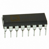
IC SRL DAC 12BIT LC2MOS 16-DIP
Manufacturer
Analog Devices Inc
Series
DACPORT®r
Datasheet
1.AD7243ANZ.pdf
(12 pages)
Specifications of AD7243AN
Data Interface
Serial
Settling Time
10µs
Rohs Status
RoHS non-compliant
Number Of Bits
12
Number Of Converters
1
Voltage Supply Source
Dual ±
Power Dissipation (max)
100mW
Operating Temperature
-40°C ~ 85°C
Mounting Type
Through Hole
Package / Case
16-DIP (0.300", 7.62mm)
Resolution (bits)
12bit
Digital Ic Case Style
DIP
No. Of Pins
16
Operating Temperature Range
-40°C To +85°C
Update Rate
0.1MSPS
Package
16PDIP
Resolution
12 Bit
Conversion Rate
300 KSPS
Architecture
R-2R
Digital Interface Type
Serial (3-Wire)
Number Of Outputs Per Chip
1
Output Type
Voltage
Full Scale Error
±6 LSB
Integral Nonlinearity Error
±1 LSB
Maximum Settling Time
10 us
Number Of Channels
1
Interface Type
Serial (3-Wire)
Single Supply Voltage (typ)
12/15V
Dual Supply Voltage (typ)
±12/±15V
Power Supply Requirement
Single/Dual
Single Supply Voltage (min)
10.8V
Single Supply Voltage (max)
16.5V
Dual Supply Voltage (min)
±10.8V
Dual Supply Voltage (max)
±16.5V
Operating Temp Range
-40C to 85C
Operating Temperature Classification
Industrial
Mounting
Through Hole
Pin Count
16
Package Type
PDIP
Lead Free Status / Rohs Status
Not Compliant
Available stocks
Company
Part Number
Manufacturer
Quantity
Price
Company:

Part Number:
AD7243AN
Manufacturer:
AD
Quantity:
5 510
Company:
Part Number:
AD7243ANZ
Manufacturer:
AMTEL
Quantity:
648
Part Number:
AD7243ANZ
Manufacturer:
ADI/亚德诺
Quantity:
20 000


CAUTION
ESD (electrostatic discharge) sensitive device. Electrostatic charges as high as 4000 V readily
accumulate on the human body and test equipment and can discharge without detection. Although
the AD7243 features proprietary ESD protection circuitry, permanent damage may occur on
devices subjected to high-energy electrostatic discharges. Therefore, proper ESD precautions are
recommended to avoid performance degradation or loss of functionality.
TIMING CHARACTERISTICS
AD7243AN
AD7243BN
AD7243AR
AD7243BR
AD7243AQ
AD7243BQ
AD7243SQ
NOTES
1
2
ABSOLUTE MAXIMUM RATINGS
(T
V
V
AGND to DGND . . . . . . . . . . . . . . . . –0.3 V to V
V
REFOUT to AGND . . . . . . . . . . . . . . . . . . . . . . . 0 V to V
REFIN to AGND . . . . . . . . . . . . . . . . –0.3 V to V
Digital Inputs to DGND . . . . . . . . . . . –0.3 V to V
SDO to DGND . . . . . . . . . . . . . . . . . . –0.3 V to V
Operating Temperature Range
Parameter
t
t
t
t
t
t
t
t
t
t
t
NOTES
1
2
3
4
5
6
Model
N = Plastic DIP; R = SOIC; Q = Cerdip.
Available to /883B processing only. Contact your local sales office for military data sheet.
Sample tested at +25°C to ensure compliance. All input signals are specified with tr = tf = 5 ns (10% to 90% of 5 V) and timed from a voltage level of 1.6 V.
See Figures 7 & 8.
SCLK mark/space ratio range is 40/60 to 60/40.
SDO load capacitance is no greater than 50 pF.
At 25°C t
Guaranteed by design.
1
2
3
4
5
6
7
8
9
10
11
DD
SS
OUT
3
A
Industrial (A, B Versions) . . . . . . . . . . . . . –40°C to +85°C
Extended (S Version) . . . . . . . . . . . . . . . . –55°C to +125°C
4, 5
4, 6
= +25°C unless otherwise noted)
to AGND, DGND . . . . . . . . . . . . . . . . . +0.3 V to –17 V
to AGND, DGND . . . . . . . . . . . . . . . . . –0.3 V to +17 V
2
to AGND . . . . . . . . . . . . . . . . . . . –6 V to V
10
is 130 ns max.
2
Limit at +25 C, T
(All Versions)
200
15
70
0
40
0
20
0
20
160
>t
5
Temperature Range
–40°C to +85°C
–40°C to +85°C
–40°C to +85°C
–40°C to +85°C
–40°C to +85°C
–40°C to +85°C
–55°C to +125°C
MIN
1
1, 2
, T
MAX
(V
R
L
DD
= 2 k , C
= +10.8 V to +16.5 V, V
DD
DD
DD
DD
DD
Units
ns min
ns min
ns min
ns min
ns min
ns min
ns min
ns min
ns min
ns max
ns min
ORDERING GUIDE
+ 0.3 V
+ 0.3 V
+ 0.3 V
+ 0.3 V
+ 0.3 V
L
= 100 pF. All Specifications T
DD
Storage Temperature Range . . . . . . . . . . . . –65°C to +150°C
Lead Temperature (Soldering, 10 secs) . . . . . . . . . . . . +300°C
Power Dissipation (Any Package) to +75°C . . . . . . . 450 mW
Derates above +75°C by . . . . . . . . . . . . . . . . . . . . . 6 mW/°C
NOTES
1
2
Stresses above those listed under Absolute Maximum Ratings may cause perma-
nent damage to the device. This is a stress rating only; functional operation of the
device at these or any other conditions above those listed in the operational sections
of this specification is not implied. Exposure to absolute maximum rating condi-
tions for extended periods may affect device reliability. Only one Absolute
Maximum Rating may be applied at any time.
The outputs may be shorted to voltages in this range provided the power dissipation
of the package is not exceeded. Short circuit current is typically 80 mA.
Conditions/Comments
SCLK Cycle Time
SYNC to SCLK Falling Edge Setup Time
SYNC to SCLK Hold Time
Data Setup Time
Data Hold Time
SYNC High to LDAC Low
LDAC Pulsewidth
LDAC High to SYNC Low
CLR Pulsewidth
SCLK Falling Edge to SDO Valid
SCLK Falling Edge to SDO Invalid
SS
= 0 V or –10.8 V to –16.5 V, AGND = DGND = 0 V,
Relative Accuracy
± 1 LSB
± 1/2 LSB
± 1 LSB
± 1/2 LSB
± 1 LSB
± 1/2 LSB
± 1 LSB
MIN
to T
MAX
unless otherwise noted.)
WARNING!
Package Option
N-16
N-16
R-16
R-16
Q-16
Q-16
Q-16
ESD SENSITIVE DEVICE
AD7243
1
Related parts for AD7243AN
Image
Part Number
Description
Manufacturer
Datasheet
Request
R

Part Number:
Description:
±1.7g Dual-Axis IMEMS Accelerometer Evaluation Board
Manufacturer:
Analog Devices Inc
Datasheet:

Part Number:
Description:
Inertial Sensor Evaluation System
Manufacturer:
Analog Devices Inc
Datasheet:
Part Number:
Description:
Manufacturer:
Analog Devices Inc
Datasheet:
Part Number:
Description:
Manufacturer:
Analog Devices Inc
Datasheet:
Part Number:
Description:
Manufacturer:
Analog Devices Inc
Datasheet:
Part Number:
Description:
Manufacturer:
Analog Devices Inc
Datasheet:
Part Number:
Description:
Manufacturer:
Analog Devices Inc
Datasheet:
Part Number:
Description:
Manufacturer:
Analog Devices Inc
Datasheet:
Part Number:
Description:
Manufacturer:
Analog Devices Inc
Datasheet:
Part Number:
Description:
Manufacturer:
Analog Devices Inc
Datasheet:
Part Number:
Description:
Manufacturer:
Analog Devices Inc
Datasheet:
Part Number:
Description:
Manufacturer:
Analog Devices Inc
Datasheet:
Part Number:
Description:
Manufacturer:
Analog Devices Inc
Datasheet: