AD7243AN Analog Devices Inc, AD7243AN Datasheet - Page 8
AD7243AN
Manufacturer Part Number
AD7243AN
Description
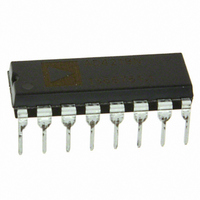
IC SRL DAC 12BIT LC2MOS 16-DIP
Manufacturer
Analog Devices Inc
Series
DACPORT®r
Datasheet
1.AD7243ANZ.pdf
(12 pages)
Specifications of AD7243AN
Data Interface
Serial
Settling Time
10µs
Rohs Status
RoHS non-compliant
Number Of Bits
12
Number Of Converters
1
Voltage Supply Source
Dual ±
Power Dissipation (max)
100mW
Operating Temperature
-40°C ~ 85°C
Mounting Type
Through Hole
Package / Case
16-DIP (0.300", 7.62mm)
Resolution (bits)
12bit
Digital Ic Case Style
DIP
No. Of Pins
16
Operating Temperature Range
-40°C To +85°C
Update Rate
0.1MSPS
Package
16PDIP
Resolution
12 Bit
Conversion Rate
300 KSPS
Architecture
R-2R
Digital Interface Type
Serial (3-Wire)
Number Of Outputs Per Chip
1
Output Type
Voltage
Full Scale Error
±6 LSB
Integral Nonlinearity Error
±1 LSB
Maximum Settling Time
10 us
Number Of Channels
1
Interface Type
Serial (3-Wire)
Single Supply Voltage (typ)
12/15V
Dual Supply Voltage (typ)
±12/±15V
Power Supply Requirement
Single/Dual
Single Supply Voltage (min)
10.8V
Single Supply Voltage (max)
16.5V
Dual Supply Voltage (min)
±10.8V
Dual Supply Voltage (max)
±16.5V
Operating Temp Range
-40C to 85C
Operating Temperature Classification
Industrial
Mounting
Through Hole
Pin Count
16
Package Type
PDIP
Lead Free Status / Rohs Status
Not Compliant
Available stocks
Company
Part Number
Manufacturer
Quantity
Price
Company:

Part Number:
AD7243AN
Manufacturer:
AD
Quantity:
5 510
Company:
Part Number:
AD7243ANZ
Manufacturer:
AMTEL
Quantity:
648
Part Number:
AD7243ANZ
Manufacturer:
ADI/亚德诺
Quantity:
20 000


APPLYING THE AD7243
Power Supply Decoupling
To achieve optimum performance when using the AD7243, the
V
0.1 µF capacitors. In noisy environments it is recommended
that 10 µF capacitors be connected in parallel with the 0.1 µF
capacitors.
The internal scaling resistors provided on the AD7243 allow
several output voltage ranges. The part can produce unipolar
output ranges of 0 V to +5 V or 0 V to +10 V and a bipolar out-
put range of ± 5 V. Connections for the various ranges are out-
lined below.
Unipolar (0 V to +10 V) Configuration
The first of the configurations provides an output voltage range
of 0 V to +10 V. This is achieved by connecting the output off-
set resistor R
is selected by connecting BIN/COMP (Pin 4) to DGND. In this
configuration, the AD7243 can be operated using either single
or dual supplies. Note that the V
for this range in order to maintain sufficient amplifier head-
room. Dual supplies may be used to improve settling time and
give increased current sink capability for the amplifier. Figure 9
shows the connection diagram for unipolar operation of the
AD7243. Table I shows the digital code vs. analog output for
this configuration.
Input Data Word
XXXX 1111 1111 1111 +2 REFIN × (4095/4096)
XXXX 1000 0000 0001 +2 REFIN × (2049/4096)
XXXX 1000 0000 0000 +2 REFIN × (2048/4096) = +REFIN
XXXX 0111 1111 1111 +2 REFIN × (2047/4096)
XXXX 0000 0000 0001 +2 REFIN × (1/4096)
XXXX 0000 0000 0000 0 V
X = Don’t Care.
Note: 1 LSB = 2 REFIN/4096.
AD7243
DD
REFOUT
and V
REFIN
Table I. Unipolar Code Table (0 V to +10 V Range)
MSB
SS
*ADDITIONAL PINS OMITTED FOR CLARITY
OFS
lines should each be decoupled to DGND using
(Pin 13) to AGND. Natural Binary data format
COMP
BIN/
LSB
Analog Output, V
DGND
AD7243*
DAC
DD
V
DD
V
supply must be ≥+14.25 V
DD
AGND
2R
2R
0V OR V
V
SS
OUT
V
R
0V TO + 10V
OUT
OFS
SS
Unipolar (0 V to +5 V) Configuration
The 0 V to +5 V output voltage range is achieved by connecting
R
either single or dual supplies. The table for output voltage vs.
digital code is as in Table I, with 2REFIN replaced by REFIN.
Note, for this range, 1 LSB = REFIN • (2
Bipolar ( 5 V) Configuration
The bipolar configuration for the AD7243, which gives an out-
put range of –5 V to +5 V, is achieved by connecting R
REFIN. The AD7243 must be operated from dual supplies to
achieve this output voltage range. Either offset binary or two’s
complement data format may be selected. Figure 10 shows the
connection diagram for bipolar operation. An AD586 provides
the reference voltage for the DAC but this could be provided by
the on-chip reference by connecting REFOUT to REFIN.
Bipolar Operation (Two’s Complement Data Format)
The AD7243 is configured for two’s complement data format
by connecting BIN/COMP (Pin 4) high. The analog output vs.
digital code is shown in Table II.
Input Data Word
XXXX 0111 1111 1111
XXXX 0000 0000 0001
XXXX 0000 0000 0000
XXXX 1111 1111 1111
XXXX 1000 0000 0001
XXXX 1000 0000 0000
X = Don’t Care.
Note: 1 LSB = REFIN/2048.
Bipolar Operation (Offset Binary Data Format)
The AD7243 is configured for Offset Binary data format by
connecting BIN/COMP (Pin 4) low. The analog output vs. digi-
tal code may be obtained by inverting the MSB in Table II.
OFS
GND
AD586
to V
Table II. Two’s Complement Bipolar Code Table
+V
MSB
OUT
IN
V
OUT
. Once again, the AD7243 can be operated using
REFIN
BIN/ COMP
*ADDITIONAL PINS OMITTED FOR CLARITY
LSB
+REFIN × (2047/2048)
+REFIN × (1/2048)
0 V
–REFIN × (1/2048)
–REFIN × (2047/2048)
–REFIN × (2048/2048) = –REFIN
Analog Output, V
V
DD
R
OFS
DAC
DGND
V
V
DD
DD
–12
2R
AD7243*
) = (REFIN/4096).
OUT
AGND
2R
V
SS
V
OFS
SS
V
–5V TO + 5V
to
OUT
Related parts for AD7243AN
Image
Part Number
Description
Manufacturer
Datasheet
Request
R

Part Number:
Description:
±1.7g Dual-Axis IMEMS Accelerometer Evaluation Board
Manufacturer:
Analog Devices Inc
Datasheet:

Part Number:
Description:
Inertial Sensor Evaluation System
Manufacturer:
Analog Devices Inc
Datasheet:
Part Number:
Description:
Manufacturer:
Analog Devices Inc
Datasheet:
Part Number:
Description:
Manufacturer:
Analog Devices Inc
Datasheet:
Part Number:
Description:
Manufacturer:
Analog Devices Inc
Datasheet:
Part Number:
Description:
Manufacturer:
Analog Devices Inc
Datasheet:
Part Number:
Description:
Manufacturer:
Analog Devices Inc
Datasheet:
Part Number:
Description:
Manufacturer:
Analog Devices Inc
Datasheet:
Part Number:
Description:
Manufacturer:
Analog Devices Inc
Datasheet:
Part Number:
Description:
Manufacturer:
Analog Devices Inc
Datasheet:
Part Number:
Description:
Manufacturer:
Analog Devices Inc
Datasheet:
Part Number:
Description:
Manufacturer:
Analog Devices Inc
Datasheet:
Part Number:
Description:
Manufacturer:
Analog Devices Inc
Datasheet: