AD7243AN Analog Devices Inc, AD7243AN Datasheet - Page 9
AD7243AN
Manufacturer Part Number
AD7243AN
Description
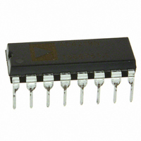
IC SRL DAC 12BIT LC2MOS 16-DIP
Manufacturer
Analog Devices Inc
Series
DACPORT®r
Datasheet
1.AD7243ANZ.pdf
(12 pages)
Specifications of AD7243AN
Data Interface
Serial
Settling Time
10µs
Rohs Status
RoHS non-compliant
Number Of Bits
12
Number Of Converters
1
Voltage Supply Source
Dual ±
Power Dissipation (max)
100mW
Operating Temperature
-40°C ~ 85°C
Mounting Type
Through Hole
Package / Case
16-DIP (0.300", 7.62mm)
Resolution (bits)
12bit
Digital Ic Case Style
DIP
No. Of Pins
16
Operating Temperature Range
-40°C To +85°C
Update Rate
0.1MSPS
Package
16PDIP
Resolution
12 Bit
Conversion Rate
300 KSPS
Architecture
R-2R
Digital Interface Type
Serial (3-Wire)
Number Of Outputs Per Chip
1
Output Type
Voltage
Full Scale Error
±6 LSB
Integral Nonlinearity Error
±1 LSB
Maximum Settling Time
10 us
Number Of Channels
1
Interface Type
Serial (3-Wire)
Single Supply Voltage (typ)
12/15V
Dual Supply Voltage (typ)
±12/±15V
Power Supply Requirement
Single/Dual
Single Supply Voltage (min)
10.8V
Single Supply Voltage (max)
16.5V
Dual Supply Voltage (min)
±10.8V
Dual Supply Voltage (max)
±16.5V
Operating Temp Range
-40C to 85C
Operating Temperature Classification
Industrial
Mounting
Through Hole
Pin Count
16
Package Type
PDIP
Lead Free Status / Rohs Status
Not Compliant
Available stocks
Company
Part Number
Manufacturer
Quantity
Price
Company:

Part Number:
AD7243AN
Manufacturer:
AD
Quantity:
5 510
Company:
Part Number:
AD7243ANZ
Manufacturer:
AMTEL
Quantity:
648
Part Number:
AD7243ANZ
Manufacturer:
ADI/亚德诺
Quantity:
20 000


MICROPROCESSOR INTERFACING
Microprocessor interfacing to the AD7243 is via a serial bus
which uses standard protocol compatible with DSP processors
and microcontrollers. The communications channel requires a
three-wire interface consisting of a clock signal, a data signal
and a synchronization signal. The AD7243 requires a 16-bit
data word with data valid on the falling edge of SCLK. For all
the interfaces, the DAC update may be done automatically
when all the data is clocked in or it may be done under control
of LDAC.
Figures 11 to 16 show the AD7243 configured for interfacing to
a number of popular DSP processors and microcontrollers.
AD7243–ADSP-2101/ADSP-2102 Interface
Figure 11 shows a serial interface between the AD7243 and the
ADSP-2101/ADSP-2102 DSP processor. The ADSP-2101/
ADSP-2102 contains two serial ports, and either port may be
used in the interface. The data transfer is initiated by TFS going
low. Data from the ADSP-2101/ADSP-2102 is clocked into the
AD7243 on the falling edge of SCLK. When the data transfer is
complete, TFS is taken high. In the interface shown the DAC is
updated using an external timer which generates an LDAC
pulse. This could also be done using a control or decoded ad-
dress line from the processor. Alternatively, the LDAC input
could be hard wired low and in this case the update takes place
automatically on the sixteenth falling edge of SCLK.
*ADDITIONAL PINS OMITTED FOR CLARITY
ADSP - 2101/
ADSP - 2102*
SCLK
TFS
DT
TIMER
SCLK
SDIN
LDAC
SYNC
AD7243*
AD7243–DSP56000 Interface
A serial interface between the AD7243 and the DSP56000 is
shown in Figure 12. The DSP56000 is configured for Normal
Mode Asynchronous operation with Gated Clock. It is also set
up for a 16-bit word with SCK and SC2 as outputs and the FSL
control bit set to a “0.” SCK is internally generated on the
DSP56000 and applied to the AD7243 SCLK input. Data from
the DSP56000 is valid on the falling edge of SCK. The SC2
output provides the framing pulse for valid data. This line must
be inverted before being applied to the SYNC input of the
AD7243.
The LDAC input of the AD7243 is connected to DGND so the
update of the DAC latch takes place automatically on the six-
teenth falling edge of SCLK. An external timer could also be
used as in the previous interface if an external update is
required.
AD7243–TMS32020 Interface
Figure 13 shows a serial interface between the AD7243 and the
TMS32020 DSP processor. In this interface, the CLKX and
FSX signals for the TMS32020 should be generated using ex-
ternal clock/timer circuitry. The FSX pin of the TMS32020
must be configured as an input. Data from the TMS32020 is
valid on the falling edge of CLKX.
The clock/timer circuitry generates the LDAC signal for the
AD7243 to synchronize the update of the output with the serial
transmission. Alternatively, the automatic update mode may be
selected by connecting LDAC to DGND.
*ADDITIONAL PINS OMITTED FOR CLARITY
*ADDITIONAL PINS OMITTED FOR CLARITY
TMS32020
DSP56000
CLKX
SCK
STD
SC2
FSX
DX
CLOCK/
TIMER
SCLK
SDIN
LDAC
SYNC
LDAC
SYNC
SCLK
SDIN
AD7243*
AD7243*
AD7243
Related parts for AD7243AN
Image
Part Number
Description
Manufacturer
Datasheet
Request
R

Part Number:
Description:
±1.7g Dual-Axis IMEMS Accelerometer Evaluation Board
Manufacturer:
Analog Devices Inc
Datasheet:

Part Number:
Description:
Inertial Sensor Evaluation System
Manufacturer:
Analog Devices Inc
Datasheet:
Part Number:
Description:
Manufacturer:
Analog Devices Inc
Datasheet:
Part Number:
Description:
Manufacturer:
Analog Devices Inc
Datasheet:
Part Number:
Description:
Manufacturer:
Analog Devices Inc
Datasheet:
Part Number:
Description:
Manufacturer:
Analog Devices Inc
Datasheet:
Part Number:
Description:
Manufacturer:
Analog Devices Inc
Datasheet:
Part Number:
Description:
Manufacturer:
Analog Devices Inc
Datasheet:
Part Number:
Description:
Manufacturer:
Analog Devices Inc
Datasheet:
Part Number:
Description:
Manufacturer:
Analog Devices Inc
Datasheet:
Part Number:
Description:
Manufacturer:
Analog Devices Inc
Datasheet:
Part Number:
Description:
Manufacturer:
Analog Devices Inc
Datasheet:
Part Number:
Description:
Manufacturer:
Analog Devices Inc
Datasheet: