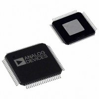
AD9726BSVZ Analog Devices Inc, AD9726BSVZ Datasheet

AD9726BSVZ
Specifications of AD9726BSVZ
Available stocks
Related parts for AD9726BSVZ
AD9726BSVZ Summary of contents
Page 1
FEATURES Dynamic performance SFDR ≥ 78 dBc MHz OUT IMD ≥ 82 dBc MHz OUT ACLR ≥ 76 dBc MHz OUT NSD ≤ −160 dB/ ...
Page 2
AD9726 TABLE OF CONTENTS Features .............................................................................................. 1 Applications ....................................................................................... 1 Functional Block Diagram .............................................................. 1 General Description ......................................................................... 1 Product Highlights ........................................................................... 1 Revision History ............................................................................... 2 Specifications ..................................................................................... 3 DC Specifications ......................................................................... 3 AC Specifications .......................................................................... 4 Digital Signal ...
Page 3
SPECIFICATIONS DC SPECIFICATIONS DBVDD = AVDD1 = AVDD2 = 3.3 V, DVDD = CLKVDD = ADVDD = ACVDD = 2 unless otherwise specified. MIN MAX Table 1. Parameter 1 ACCURACY DNL INL Offset Error ...
Page 4
AD9726 AC SPECIFICATIONS DBVDD = AVDD1 = AVDD2 = 3.3 V, DVDD = CLKVDD = ADVDD = ACVDD = 2 unless otherwise specified. MIN MAX Table 2. Parameter DYNAMIC PERFORMANCE Output Settling Time (t ...
Page 5
DIGITAL SIGNAL SPECIFICATIONS DBVDD = AVDD1 = AVDD2 = 3.3 V, DVDD = CLKVDD = ADVDD = ACVDD = 2 unless otherwise specified. MIN MAX Table 3. Parameter DAC CLOCK INPUTS (CLK±) Differential Voltage ...
Page 6
AD9726 Parameter SERIAL PORT INTERFACE SCLK Frequency (f ) SCLK SCLK Rise/Fall Time SCLK Pulse Width High (t ) CPWH SCLK Pulse Width Low (t ) CPWL SCLK Setup Time (t ) CSU SDIO Setup Time (t ) DSU SDIO ...
Page 7
DB0 TO DB15 CLK+/CLK– PIPE-BYPASS PD-BYPASS IOUTA OR IOUTB Figure 5. Data Synchronization Bypass Pipeline Delay CSB SCLK SET-UP TIME t CSU SCLK PULSE WIDTH HIGH/LOW TIME t CPWH SCLK SDIO SET-UP TIME SDIO HOLD TIME t ...
Page 8
AD9726 ABSOLUTE MAXIMUM RATINGS Table 5. Parameter With Respect to DBVDD, AVDD1, DBGND, AGND1, AVDD2 AGND2 DVDD, CLKVDD, DGND, CLKGND, ACVDD, ADVDD ACGND, ADGND DBGND, AGND1, DBGND, AGND1, AGND2 AGND2 DGND, CLKGND, DGND, CLKGND, ACGND, ADGND ACGND, ADGND REFIO, FSDAJ ...
Page 9
PIN CONFIGURATION AND FUNCTION DESCRIPTIONS CLKVDD 1 REXT 2 CLKVDD 3 CLKGND 4 CLK+ 5 CLK– 6 CLKGND 7 DGND ...
Page 10
AD9726 Pin No. Mnemonic Description 43 DB4− Data Bit 4 Complement 44 DB3+ Data Bit 3 True 45 DB3− Data Bit 3 Complement 46 DB2+ Data Bit 2 True 47 DB2− Data Bit 2 Complement 48 DB1+ Data Bit 1 ...
Page 11
TERMINOLOGY Integral Nonlinearity (INL) The maximum deviation of the actual analog output from the ideal output, as determined by a straight line drawn from zero scale to full scale. Differential Nonlinearity (DNL) A measure of the maximum deviation in analog ...
Page 12
AD9726 TYPICAL PERFORMANCE CHARACTERISTICS 100 90 –6dB 80 –3dB 70 0dB (MHz) OUT Figure 8. SFDR vs 400 MSPS OUT 100 90 –6dB 80 0dB 70 60 ...
Page 13
RBW 1kHz VBW 1kHz REF LVL SWT 17s 0dBm 0 –10 –20 –30 –40 1AVG –50 –60 –70 –80 –90 –100 –110 –120 START 750kHz 675kHz Figure 14. THD at 400 MSPS and MHz (Diplexer High-Pass Output ...
Page 14
AD9726 REF –50dBm *ATTEN 2dB *AVG Log 10dB/ PAVG CENTER 70.00MHz *RES BW 10kHz VBW 100kHz SWEEP 2.451s (601 pts) TOTAL CARRIER POWER -20.62dBm/15.3600MHz RRC FILTER: ON FILTER ALPHA 0.22 REF CARRIER POWER -26.43dBm/3.84000MHz LOWER OFFSET FREQ ...
Page 15
SERIAL PORT INTERFACE Table 8. SPI Register Map Addr Bit 7 Bit 6 0x00 SDIODIR DATADIR 0x02 DATAFMT DATARATE 0x0E 0x0F SCALSTAT SELFCAL 0x10 MEMADR[7] MEMADR[6] 0x11 0x15 0x16 BYPASS Table 9. SPI Register Bit Default and Descriptions Values Addr ...
Page 16
AD9726 Addr Name Bits I/O Default 0x10 MEMADR [7:0] I 00000000 0x11 MEMDAT [5:0] I/O 000000 0x15 SYNCOUT [1: 0x16 BYPASS SYNCEXT SYNCIN [4: SWRESET also resets itself. SMEM ...
Page 17
THEORY OF OPERATION The AD9726 uses LVDS for input data to enable high sample rates and high performance. LVDS technology uses differential signals for noise rejection and small signal amplitude for fast speed with lower power. Each LVDS input on ...
Page 18
AD9726 The 50 Ω termination resistor should be placed as close as pos- sible to the input pins, and controlled impedance PCB traces should be used. Good ac performance can be expected from either the active or passive DAC clock ...
Page 19
INTERNAL REFERENCE AND FULL-SCALE OUTPUT The AD9726 contains an internal 1.2 V precision reference source; this reference voltage appears at the REFIO pin. It can be used to drive external circuitry if properly buffered. Apply an external reference voltage source ...
Page 20
AD9726 MSB/LSB Transfers The SPI can support both MSB- and LSB-justified serial data byte formats. This functionality is determined by Bit 6 in SPI Register 0x00. This bit defaults low, which is MSB justification. In this mode, serial data bits ...
Page 21
Linearity CALDACs operate inversely from their input; that is, as their binary input value increases, the magnitude of their current contribution seen at the AD9726 output decreases. Gain CALDACs are an exception to this. Their contribution seen at the AD9726 ...
Page 22
AD9726 and the SELFCAL bit is cleared. Following the cycle, the device reports a self-calibrated state (CALMEM = 01b). As with MEMXFER, successful assertion of the SELFCAL bit (Bit 6 in Register 0x0F)requires that Bits[3:0] in Register 0x0F be clear. ...
Page 23
SYNCUPD at the next convenient time. In manual mode, users can choose when to update the sync logic. When operating with burst data, issuing a sync update between active bursts updates the system ...
Page 24
... Figure 24. 80-Lead Thin Plastic Quad Flat Package, Exposed Pad [TQFP_EP] ORDERING GUIDE 1 Model Temperature Range AD9726BSVZ −40°C to +85°C AD9726BSVZRL −40°C to +85°C AD9726-EBZ RoHS Compliant Part. © 2005-2010 Analog Devices, Inc. All rights reserved. Trademarks and registered trademarks are the property of their respective owners. ...


