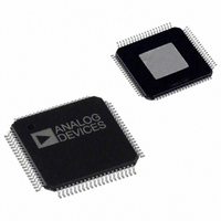
AD9726BSVZ Analog Devices Inc, AD9726BSVZ Datasheet - Page 16

AD9726BSVZ
Manufacturer Part Number
AD9726BSVZ
Description
IC DAC 16IT LVDS 400MSPS 80-TQFP
Manufacturer
Analog Devices Inc
Series
TxDAC+®r
Datasheet
1.AD9726BSVZRL.pdf
(24 pages)
Specifications of AD9726BSVZ
Data Interface
Parallel
Number Of Bits
16
Number Of Converters
1
Voltage Supply Source
Analog and Digital
Power Dissipation (max)
575mW
Operating Temperature
-40°C ~ 85°C
Mounting Type
Surface Mount
Package / Case
80-TQFP Exposed Pad, 80-eTQFP, 80-HTQFP, 80-VQFP
Resolution (bits)
16bit
Sampling Rate
400MSPS
Input Channel Type
Parallel
Supply Current
80mA
Digital Ic Case Style
QFP
No. Of Pins
80
Package
80TQFP EP
Resolution
16 Bit
Conversion Rate
400 MSPS
Digital Interface Type
Parallel
Number Of Outputs Per Chip
1
Output Type
Current
Full Scale Error
0.003(Typ) %FSR
Integral Nonlinearity Error
±2.5 LSB
Maximum Settling Time
0.0105(Typ) us
Lead Free Status / RoHS Status
Lead free / RoHS Compliant
For Use With
AD9726-EBZ - BOARD EVAL FOR AD9726
Settling Time
-
Lead Free Status / RoHS Status
Lead free / RoHS Compliant, Lead free / RoHS Compliant
Available stocks
Company
Part Number
Manufacturer
Quantity
Price
Company:
Part Number:
AD9726BSVZ
Manufacturer:
Epson
Quantity:
1 271
Company:
Part Number:
AD9726BSVZ
Manufacturer:
Analog Devices Inc
Quantity:
10 000
Company:
Part Number:
AD9726BSVZRL
Manufacturer:
Analog Devices Inc
Quantity:
10 000
AD9726
Addr
0x10
0x11
0x15
0x16
1
2
3
4
5
6
SWRESET also resets itself. SMEM contents are unaffected by SWRESET; however, CALMEM reports an uncalibrated state.
EXTREF is optional because the internal reference circuit is designed to be overdriven by an external source.
The self-calibration clock is also used for the memory transfer cycle; therefore, the CALCLK value affects the MEMXFER process time.
Register Bits 3:0 must all be 0 to assert SELFCAL. The time required for the self-calibration cycle is ~100 ms at 100 MHz with CALCLK = 0.
Register Bits 3:0 must all be 0 to assert MEMXFER. The time required for the memory transfer cycle is ~15 ms at 100 MHz with CALCLK = 0.
The UNCAL bit remains asserted after the cycle completes (SMEM contents held at default values) until the bit is cleared by the user.
Name
MEMADR
MEMDAT
SYNCOUT
BYPASS
SYNCEXT
SYNCIN
Bits
[7:0]
[5:0]
[1:0]
6
5
[4:3]
I/O
I
I/O
O
I
I
I
Default
00000000
000000
00
0
0
00
Description
8-bit memory address value for read/write operations.
6-bit memory data value for read/write operations.
2-bit output value indicates current sync quadrant.
1: bypasses data synchronization circuitry. Data is sampled using the DAC clock (CLK±)
1: enables sync external mode; disable auto quadrant select.
2-bit input value is used to specify the sync quadrant.
Rev. B | Page 16 of 24


