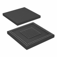
ADSP-BF527KBCZ-6C2 Analog Devices Inc, ADSP-BF527KBCZ-6C2 Datasheet - Page 11

ADSP-BF527KBCZ-6C2
Manufacturer Part Number
ADSP-BF527KBCZ-6C2
Description
IC DSP 16BIT 600MHZ 289CSPBGA
Manufacturer
Analog Devices Inc
Series
Blackfin®r
Type
Fixed Pointr
Datasheets
1.ADSP-BF531SBSTZ400.pdf
(12 pages)
2.ADSP-BF523BBCZ-5A.pdf
(88 pages)
3.ADSP-BF523KBCZ-5C2.pdf
(36 pages)
Specifications of ADSP-BF527KBCZ-6C2
Package / Case
289-CSPBGA
Interface
DMA, Ethernet, I²C, PPI, SPI, SPORT, UART, USB
Clock Rate
600MHz
Non-volatile Memory
ROM (32 kB)
On-chip Ram
132kB
Voltage - I/o
1.8V, 2.5V, 3.3V
Voltage - Core
1.10V
Operating Temperature
0°C ~ 70°C
Mounting Type
Surface Mount
Svhc
No SVHC (18-Jun-2010)
Cache On Chip L1/l2 Memory
48KB
Core Frequency Typ
600MHz
Dsp Type
Core
External Supported Memory
SDRAM, SRAM, FLASH, ROM
Interface Type
SPI, Parallel, 2 Wire
Rohs Compliant
Yes
Mmac
1200
No. Of Pins
289
Package
289CSP-BGA
Maximum Speed
600 MHz
Lead Free Status / RoHS Status
Lead free / RoHS Compliant
For Use With
ADZS-BF527-MPSKIT - BOARD EVAL MEDIA PLAYER BF527ADZS-BF527-EZLITE - BOARD EVAL ADSP-BF527
Lead Free Status / RoHS Status
Lead free / RoHS Compliant, Lead free / RoHS Compliant
Available stocks
Company
Part Number
Manufacturer
Quantity
Price
Company:
Part Number:
ADSP-BF527KBCZ-6C2
Manufacturer:
Analog Devices Inc
Quantity:
10 000
SOFTWARE CONTROL INTERFACE
The software control interface provides access to the
programmer-selectable control registers and can operate with a
2-wire (TWI) or 3-wire (SPI) interface, depending on the setting
of the CMODE pin. If the CMODE pin is set to 0, the 2-wire
interface is selected; if 1, the 3-wire interface is selected.
Within each control register is a control data-word consisting of
16 bits, MSB first. Bit B15 to Bit B9 are the register map address,
and Bit B8 to Bit B0 are register data for the associated register
map.
ADSP-BF522C/ADSP-BF523C/ADSP-BF524C/ADSP-BF525C/ADSP-BF526C/ADSP-BF527C
A(M) = ACKNOWLEDGE BY MASTER.
A(M) = ACKNOWLEDGE BY MASTER (INVERSION).
A(S) = ACKNOWLEDGE BY SLAVE.
S/P = START/STOP BIT.
A0 = I
SEQUENCE
SEQUENCE
WRITE
2
READ
C R/W BIT.
CSDA
S
S
CSCL
CSB
A7
A7
ADDRESS
ADDRESS
DEVICE
DEVICE
CSDA
CSCL
B15
...
...
A1
A1
B14
START
A0
0
A0
0
S
B13
REGISTER MAP
A(S)
ADDRESS
A(S)
ADDR
1 – 7
B12
B15
B15
REGISTER
REGISTER
ADDRESS
ADDRESS
B11
R/W
8
...
...
Figure 13. Codec TWI Write and Read Sequences
B10
B9
B9
Rev. A | Page 11 of 36 | March 2010
ACK
9
Figure 12. Codec TWI Serial Interface
Figure 11. Codec SPI Serial Interface
B09
B8
0
A(S)
A(S)
B08
SUBADDRESS
REGISTER
1 – 7
DATA
B07
B7
S
...
A7
B06
8
ADDRESS
DEVICE
B0
...
ACK
When 2-wire (TWI) mode is selected, CSDA generates the serial
control data-word; CSCL clocks the serial data; and CSB deter-
mines the TWI device address. If the CSB pin is set to 0, the
address selected is 0011010; if 1, the address is 0011011.
When 3-wire (SPI) mode is selected, CSDA generates the con-
trol data-word, CSCL clocks the control data-word into the
codec, and CSB latches in the control data-word.
B05
9
REGISTER
A(S)
A1
DATA
B04
A0
1
P
DATA
B03
1 – 7
A(S)
B02
B7
8
B01
...
ACK
9
B0
B0
(SLAVE DRIVE)
A(M)
REGISTER
DATA
STOP
P
0
...
0
B8
A(M)
P


