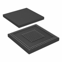
ADSP-BF527KBCZ-6C2 Analog Devices Inc, ADSP-BF527KBCZ-6C2 Datasheet - Page 3

ADSP-BF527KBCZ-6C2
Manufacturer Part Number
ADSP-BF527KBCZ-6C2
Description
IC DSP 16BIT 600MHZ 289CSPBGA
Manufacturer
Analog Devices Inc
Series
Blackfin®r
Type
Fixed Pointr
Datasheets
1.ADSP-BF531SBSTZ400.pdf
(12 pages)
2.ADSP-BF523BBCZ-5A.pdf
(88 pages)
3.ADSP-BF523KBCZ-5C2.pdf
(36 pages)
Specifications of ADSP-BF527KBCZ-6C2
Package / Case
289-CSPBGA
Interface
DMA, Ethernet, I²C, PPI, SPI, SPORT, UART, USB
Clock Rate
600MHz
Non-volatile Memory
ROM (32 kB)
On-chip Ram
132kB
Voltage - I/o
1.8V, 2.5V, 3.3V
Voltage - Core
1.10V
Operating Temperature
0°C ~ 70°C
Mounting Type
Surface Mount
Svhc
No SVHC (18-Jun-2010)
Cache On Chip L1/l2 Memory
48KB
Core Frequency Typ
600MHz
Dsp Type
Core
External Supported Memory
SDRAM, SRAM, FLASH, ROM
Interface Type
SPI, Parallel, 2 Wire
Rohs Compliant
Yes
Mmac
1200
No. Of Pins
289
Package
289CSP-BGA
Maximum Speed
600 MHz
Lead Free Status / RoHS Status
Lead free / RoHS Compliant
For Use With
ADZS-BF527-MPSKIT - BOARD EVAL MEDIA PLAYER BF527ADZS-BF527-EZLITE - BOARD EVAL ADSP-BF527
Lead Free Status / RoHS Status
Lead free / RoHS Compliant, Lead free / RoHS Compliant
Available stocks
Company
Part Number
Manufacturer
Quantity
Price
Company:
Part Number:
ADSP-BF527KBCZ-6C2
Manufacturer:
Analog Devices Inc
Quantity:
10 000
GENERAL DESCRIPTION
This document describes the differences between the
ADSP-BF52xC and the ADSP-BF52x standard Blackfin
uct. Please refer to the published ADSP-BF52x data sheet for
general description and specifications. This document only
describes the differences from that data sheet.
The ADSP-BF52xC processors add a low power, high quality
stereo audio codec for portable digital audio applications with
one set of stereo programmable gain amplifier (PGA) line
inputs and one monaural microphone input. It features two 24-
bit analog-to-digital converter (ADC) channels and two 24-bit
digital-to-analog (DAC) converter channels.
The codec can operate as a master or a slave. It supports various
master clock frequencies, including 12 MHz or 24 MHz for USB
devices; standard 256 × f
12.288 MHz and 24.576 MHz; and many common audio sam-
pling rates, such as 96 kHz, 88.2 kHz, 48 kHz, 44.1 kHz, 32 kHz,
24 kHz, 22.05 kHz, 16 kHz, 12 kHz, 11.025 kHz, and 8 kHz.
The codec can operate at power supplies as low as 1.8 V for the
analog circuitry and as low as 1.8 V for the digital circuitry. The
maximum voltage supply is 3.6 V for all supplies.
ADSP-BF522C/ADSP-BF523C/ADSP-BF524C/ADSP-BF525C/ADSP-BF526C/ADSP-BF527C
MICBIAS
RLINEIN
LLINEIN
AGND
MICIN
AVDD
VMID
OSCPD
OSC
XTO
VOLUME
VOLUME
S
or 384 × f
MIC
BOOST
CLKIN
DIVIDER
S
based rates, such as
MUTE
MUTE
MUTE
MUTE
MUX
MUX
CLKOUT
DIVIDER
Rev. A | Page 3 of 36 | March 2010
ADC
ADC
®
Figure 1. Codec Block Diagram
prod-
CSB
DIGITAL AUDIO INTERFACE
CONTROL INTERFACE
CSDA
DIGITAL
FILTERS
CSCL CMODE
The codec software-programmable stereo output options
provide the programmer with many application possibilities
because the device can be used as a headphone driver or as a
speaker driver. Its volume control functions provide a large
range of gain control of the audio signal.
CODEC DESCRIPTION
The ADSP-BF52xC codec contains a central clock source, called
the codec master clock (CODEC_MCLK) that produces a refer-
ence clock for all internal audio data processing and synch-
ronization. When using an external clock source to drive the
CODEC_MCLK pin, care should be taken to select a clock
source with less than 50 ps of jitter. Without careful generation
of the CODEC_MCLK signal, the digital audio quality
will suffer.
To enable the codec to generate the central reference clock
in a system, connect a crystal oscillator between the XTI/
CODEC_MCLK input pin and the XTO output pin.
DAC
DAC
MUTE
ATTEN/
MUTE
MUTE
MUTE
ATTEN/
MUTE
MUTE
Σ
Σ
VOLUME/
MUTE
VOLUME/
MUTE
CODEC
HEADPHONE
DRIVER
HEADPHONE
DRIVER
HPVDD
HPGND
RHPOUT
ROUT
LOUT
LHPOUT


