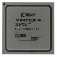
XC4VFX12-10FFG668C Xilinx Inc, XC4VFX12-10FFG668C Datasheet - Page 188

XC4VFX12-10FFG668C
Manufacturer Part Number
XC4VFX12-10FFG668C
Description
IC FPGA VIRTEX-4 FX 12K 668FCBGA
Manufacturer
Xilinx Inc
Series
Virtex™-4r
Datasheets
1.XC4VFX12-10FFG668C.pdf
(58 pages)
2.XC4VFX12-10FFG668C.pdf
(9 pages)
3.XC4VFX12-10FFG668C.pdf
(406 pages)
Specifications of XC4VFX12-10FFG668C
Total Ram Bits
663552
Number Of Logic Elements/cells
12312
Number Of Labs/clbs
1368
Number Of I /o
320
Voltage - Supply
1.14 V ~ 1.26 V
Mounting Type
Surface Mount
Operating Temperature
-40°C ~ 100°C
Package / Case
668-BBGA, FCBGA
No. Of Logic Blocks
12312
No. Of Macrocells
12312
No. Of Speed Grades
10
No. Of I/o's
320
Clock Management
DCM
I/o Supply Voltage
3.45V
Lead Free Status / RoHS Status
Lead free / RoHS Compliant
For Use With
HW-V4-ML403-UNI-G - EVALUATION PLATFORM VIRTEX-4HW-AFX-FF668-400 - BOARD DEV VIRTEX 4 FF668
Number Of Gates
-
Lead Free Status / RoHS Status
Lead free / RoHS Compliant, Lead free / RoHS Compliant
Other names
122-1591
XC4VFX12-10FFG668C
XC4VFX12-10FFG668C
Available stocks
Company
Part Number
Manufacturer
Quantity
Price
Company:
Part Number:
XC4VFX12-10FFG668C
Manufacturer:
Xilinx Inc
Quantity:
10 000
- XC4VFX12-10FFG668C PDF datasheet
- XC4VFX12-10FFG668C PDF datasheet #2
- XC4VFX12-10FFG668C PDF datasheet #3
- Current page: 188 of 406
- Download datasheet (6Mb)
Chapter 5: Configurable Logic Blocks (CLBs)
188
Distributed RAM and Memory (Available in SLICEM only)
The configuration options for the set and reset functionality of a register or a latch are as
follows:
•
•
•
•
•
•
•
Multiple left-hand LUTs in SLICEMs can be combined in various ways to store larger
amounts of data.
The function generators (LUTs) in SLICEM can be implemented as a 16 x 1-bit synchronous
RAM resource called a distributed RAM element. RAM elements are configurable within a
CLB to implement the following:
•
•
•
•
Distributed RAM modules are synchronous (write) resources. A synchronous read can be
implemented with a storage element in the same slice. The distributed RAM and the
No set or reset
Synchronous set
Synchronous reset
Synchronous set and reset
Asynchronous set (preset)
Asynchronous reset (clear)
Asynchronous set and reset (preset and clear)
Single-Port 16 x 4-bit RAM
Single-Port 32 x 2-bit RAM
Single-Port 64 x 1-bit RAM
Dual-Port 16 x 2-bit RAM
CLK
Figure 5-4: Register/Latch Configuration in a Slice
CE
SR
BY
BX
LUT F Output
www.xilinx.com
LUT G Output
D
CE
CK
D
CE
CK
SR REV
SR REV
FFY
FFX
FF
LATCH
FF
LATCH
Q
Q
UG070 (v2.6) December 1, 2008
Attribute
Attribute
ug070_5_04_071504
Reset Type
Virtex-4 FPGA User Guide
INIT1
INIT0
SRHIGH
SRLOW
INIT1
INIT0
SRHIGH
SRLOW
SYNC
ASYNC
YQ
XQ
R
Related parts for XC4VFX12-10FFG668C
Image
Part Number
Description
Manufacturer
Datasheet
Request
R

Part Number:
Description:
IC FPGA VIRTEX-4 FX 12K 363FCBGA
Manufacturer:
Xilinx Inc
Datasheet:

Part Number:
Description:
IC FPGA VIRTEX-4 FX 12K 363FCBGA
Manufacturer:
Xilinx Inc
Datasheet:

Part Number:
Description:
IC FPGA VIRTEX-4 FX 12K 363FCBGA
Manufacturer:
Xilinx Inc
Datasheet:

Part Number:
Description:
IC FPGA VIRTEX-4 FX 12K 668FCBGA
Manufacturer:
Xilinx Inc
Datasheet:

Part Number:
Description:
IC FPGA VIRTEX-4 FX 12K 363FCBGA
Manufacturer:
Xilinx Inc
Datasheet:

Part Number:
Description:
IC FPGA VIRTEX-4 FX 12K 363FCBGA
Manufacturer:
Xilinx Inc
Datasheet:

Part Number:
Description:
IC FPGA VIRTEX-4 FX 12K 668FCBGA
Manufacturer:
Xilinx Inc
Datasheet:

Part Number:
Description:
IC FPGA VIRTEX-4 FX 12K 668FCBGA
Manufacturer:
Xilinx Inc
Datasheet:

Part Number:
Description:
IC FPGA VIRTEX-4FX 363FCBGA
Manufacturer:
Xilinx Inc
Datasheet:

Part Number:
Description:
IC FPGA VIRTEX-4FX 668FFBGA
Manufacturer:
Xilinx Inc
Datasheet:

Part Number:
Description:
IC FPGA VIRTEX-4FX 363FCBGA
Manufacturer:
Xilinx Inc
Datasheet:

Part Number:
Description:
IC FPGA VIRTEX-4FX 668FFBGA
Manufacturer:
Xilinx Inc
Datasheet:

Part Number:
Description:
IC FPGA VIRTEX-4 FX 12K 668FCBGA
Manufacturer:
Xilinx Inc
Datasheet:

Part Number:
Description:
Virtex-4� Family / newest generation FPGA
Manufacturer:
XILINX [Xilinx, Inc]
Datasheet:

Part Number:
Description:
IC CPLD .8K 36MCELL 44-VQFP
Manufacturer:
Xilinx Inc
Datasheet:


