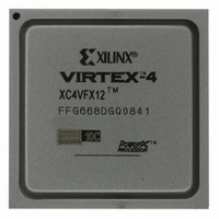
XC4VFX12-10FFG668C Xilinx Inc, XC4VFX12-10FFG668C Datasheet - Page 43

XC4VFX12-10FFG668C
Manufacturer Part Number
XC4VFX12-10FFG668C
Description
IC FPGA VIRTEX-4 FX 12K 668FCBGA
Manufacturer
Xilinx Inc
Series
Virtex™-4r
Datasheets
1.XC4VFX12-10FFG668C.pdf
(58 pages)
2.XC4VFX12-10FFG668C.pdf
(9 pages)
3.XC4VFX12-10FFG668C.pdf
(406 pages)
Specifications of XC4VFX12-10FFG668C
Total Ram Bits
663552
Number Of Logic Elements/cells
12312
Number Of Labs/clbs
1368
Number Of I /o
320
Voltage - Supply
1.14 V ~ 1.26 V
Mounting Type
Surface Mount
Operating Temperature
-40°C ~ 100°C
Package / Case
668-BBGA, FCBGA
No. Of Logic Blocks
12312
No. Of Macrocells
12312
No. Of Speed Grades
10
No. Of I/o's
320
Clock Management
DCM
I/o Supply Voltage
3.45V
Lead Free Status / RoHS Status
Lead free / RoHS Compliant
For Use With
HW-V4-ML403-UNI-G - EVALUATION PLATFORM VIRTEX-4HW-AFX-FF668-400 - BOARD DEV VIRTEX 4 FF668
Number Of Gates
-
Lead Free Status / RoHS Status
Lead free / RoHS Compliant, Lead free / RoHS Compliant
Other names
122-1591
XC4VFX12-10FFG668C
XC4VFX12-10FFG668C
Available stocks
Company
Part Number
Manufacturer
Quantity
Price
Company:
Part Number:
XC4VFX12-10FFG668C
Manufacturer:
Xilinx Inc
Quantity:
10 000
- XC4VFX12-10FFG668C PDF datasheet
- XC4VFX12-10FFG668C PDF datasheet #2
- XC4VFX12-10FFG668C PDF datasheet #3
- Current page: 43 of 406
- Download datasheet (6Mb)
Virtex-4 FPGA User Guide
UG070 (v2.6) December 1, 2008
CLR
CE
O
I
R
1
T
BUFR Use Models
BRDCK_CE
Figure 1-21: BUFR Timing Diagrams with BUFR_DIVIDE Values
The propagation delay through BUFR is different for BUFR_DIVIDE = 1 and
BUFR_DIVIDE = BYPASS. When set to 1, the delay is slightly more than BYPASS. All other
divisors have the same delay BUFR_DIVIDE = 1. The phase relationship between the input
clock and the output clock is the same for all possible divisions except BYPASS.
The timing relationship between the inputs and output of BUFR when using the
BUFR_DIVIDE attribute is illustrated in
attribute is set to three. Sometime before this diagram CLR was asserted.
In
•
•
•
•
•
BUFRs are ideal for source-synchronous applications requiring clock domain crossing or
serial-to-parallel conversion. Unlike BUFIOs, BUFRs are capable of clocking logic
resources in the FPGAs other than the IOBs.
Figure
At time T
Four clock cycles and T
the divide by three rate of the input I. T
found in the speed specification.
Note: The duty cycle is not 50/50 for odd division. The Low pulse is one cycle of I
longer.
At time event 2, CLR is asserted. After T
toggling.
At time event 3, CLR is deasserted.
At time T
rate of I.
1-21:
BRDCK_CE
BRCKO_O
after clock event 4, O begins toggling again at the divided by three
before clock event 1, CE is asserted High.
www.xilinx.com
BRCKO_O
T
BRCKO_O
after CE is asserted, the output O begins toggling at
Figure
BRCKO_O
BRDO_CLRO
Figure 1-22
1-21. In this example, the BUFR_DIVIDE
T
BRDO_CLRO
and other timing numbers are best
from time event 2, O stops
is a BUFR design example.
Regional Clocking Resources
2
3
UG070_1_21_030806
4
T
BRCKO_O
43
Related parts for XC4VFX12-10FFG668C
Image
Part Number
Description
Manufacturer
Datasheet
Request
R

Part Number:
Description:
IC FPGA VIRTEX-4 FX 12K 363FCBGA
Manufacturer:
Xilinx Inc
Datasheet:

Part Number:
Description:
IC FPGA VIRTEX-4 FX 12K 363FCBGA
Manufacturer:
Xilinx Inc
Datasheet:

Part Number:
Description:
IC FPGA VIRTEX-4 FX 12K 363FCBGA
Manufacturer:
Xilinx Inc
Datasheet:

Part Number:
Description:
IC FPGA VIRTEX-4 FX 12K 668FCBGA
Manufacturer:
Xilinx Inc
Datasheet:

Part Number:
Description:
IC FPGA VIRTEX-4 FX 12K 363FCBGA
Manufacturer:
Xilinx Inc
Datasheet:

Part Number:
Description:
IC FPGA VIRTEX-4 FX 12K 363FCBGA
Manufacturer:
Xilinx Inc
Datasheet:

Part Number:
Description:
IC FPGA VIRTEX-4 FX 12K 668FCBGA
Manufacturer:
Xilinx Inc
Datasheet:

Part Number:
Description:
IC FPGA VIRTEX-4 FX 12K 668FCBGA
Manufacturer:
Xilinx Inc
Datasheet:

Part Number:
Description:
IC FPGA VIRTEX-4FX 363FCBGA
Manufacturer:
Xilinx Inc
Datasheet:

Part Number:
Description:
IC FPGA VIRTEX-4FX 668FFBGA
Manufacturer:
Xilinx Inc
Datasheet:

Part Number:
Description:
IC FPGA VIRTEX-4FX 363FCBGA
Manufacturer:
Xilinx Inc
Datasheet:

Part Number:
Description:
IC FPGA VIRTEX-4FX 668FFBGA
Manufacturer:
Xilinx Inc
Datasheet:

Part Number:
Description:
IC FPGA VIRTEX-4 FX 12K 668FCBGA
Manufacturer:
Xilinx Inc
Datasheet:

Part Number:
Description:
Virtex-4� Family / newest generation FPGA
Manufacturer:
XILINX [Xilinx, Inc]
Datasheet:

Part Number:
Description:
IC CPLD .8K 36MCELL 44-VQFP
Manufacturer:
Xilinx Inc
Datasheet:


