EP2S30F672I4 Altera, EP2S30F672I4 Datasheet - Page 234
EP2S30F672I4
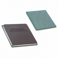
Manufacturer Part Number
EP2S30F672I4
Description
IC STRATIX II FPGA 30K 672-FBGA
Manufacturer
Altera
Series
Stratix® IIr
Datasheet
1.EP2S15F484I4N.pdf
(238 pages)
Specifications of EP2S30F672I4
Number Of Logic Elements/cells
33880
Number Of Labs/clbs
1694
Total Ram Bits
1369728
Number Of I /o
500
Voltage - Supply
1.15 V ~ 1.25 V
Mounting Type
Surface Mount
Operating Temperature
-40°C ~ 100°C
Package / Case
672-FBGA
Family Name
Stratix II
Number Of Logic Blocks/elements
33880
# I/os (max)
500
Frequency (max)
711.24MHz
Process Technology
90nm (CMOS)
Operating Supply Voltage (typ)
1.2V
Logic Cells
33880
Ram Bits
1369728
Operating Supply Voltage (min)
1.15V
Operating Supply Voltage (max)
1.25V
Operating Temp Range
-40C to 100C
Operating Temperature Classification
Industrial
Mounting
Surface Mount
Pin Count
672
Package Type
FC-FBGA
Lead Free Status / RoHS Status
Contains lead / RoHS non-compliant
Number Of Gates
-
Lead Free Status / Rohs Status
Not Compliant
Other names
544-1899
EP2S30F672I4
EP2S30F672I4
Available stocks
Company
Part Number
Manufacturer
Quantity
Price
Company:

Part Number:
EP2S30F672I4
Manufacturer:
ALTERA
Quantity:
3 000
Company:
Part Number:
EP2S30F672I4N
Manufacturer:
ALTERA
Quantity:
238


Document Revision History
5–98
Stratix II Device Handbook, Volume 1
August, 2006,
v4.2
April 2006, v4.1
December 2005,
v4.0
July 2005, v3.1
May 2005, v3.0
March 2005,
v2.2
January 2005,
v2.1
Table 5–103. Document Revision History (Part 2 of 3)
Document
Date and
Version
Updated Table 5–73, Table 5–75, Table 5–77,
Table 5–78, Table 5–79, Table 5–81, Table 5–85, and
Table 5–87.
●
●
●
●
●
●
●
●
●
●
●
●
●
●
●
●
●
●
●
●
●
●
Updated tables in “Internal Timing Parameters”
section.
Updated input rise and fall time.
Updated Table 5–3.
Updated Table 5–11.
Updated Figures 5–8 and 5–9.
Added parallel on-chip termination information to
“On-Chip Termination Specifications” section.
Updated Tables 5–28, 5–30,5–31, and 5–34.
Updated Table 5–78, Tables 5–81 through 5–90,
and Tables 5–92, 5–93, and 5–98.
Updated “PLL Timing Specifications” section.
Updated “External Memory Interface
Specifications” section.
Added Tables 5–95 and 5–101.
Updated “JTAG Timing Specifications” section,
including Figure 5–10 and Table 5–102.
Updated “External Memory Interface
Specifications” section.
Updated timing numbers throughout chapter.
Updated HyperTransport technology information in
Table 5–13.
Updated “Timing Model” section.
Updated “PLL Timing Specifications” section.
Updated “External Memory Interface
Specifications” section.
Updated tables throughout chapter.
Updated “Power Consumption” section.
Added various tables.
Replaced “Maximum Input & Output Clock Rate”
section with “Maximum Input & Output Clock Toggle
Rate” section.
Added “Duty Cycle Distortion” section.
Added “External Memory Interface Specifications”
section.
Changes Made
●
●
●
●
●
●
●
●
Changed 0.2 MHz to 2 MHz in
Table 5–93.
Added new spec for half period
jitter (Table 5–101).
Added support for PLL clock
switchover for industrial
temperature range.
Changed f
4 MHz to 2 MHz in Table 5–92.
Fixed typo in t
specification in Table 5–92.
Updated V
specifications in Table 5–28.
Updated minimum values for t
t
Update maximum values for t
t
J C L
J P Z X
, and t
Summary of Changes
, and t
I N P F D
J P S U
D I F
J P X Z
Altera Corporation
O U T J I T T E R
—
—
—
—
—
—
AC & DC max
in Table 5–102.
(min) spec from
in Table 5–102.
April 2011
J P C O
J C H
,
,
Related parts for EP2S30F672I4
Image
Part Number
Description
Manufacturer
Datasheet
Request
R

Part Number:
Description:
CYCLONE II STARTER KIT EP2C20N
Manufacturer:
Altera
Datasheet:


Part Number:
Description:
CPLD, EP610 Family, ECMOS Process, 300 Gates, 16 Macro Cells, 16 Reg., 16 User I/Os, 5V Supply, 35 Speed Grade, 24DIP
Manufacturer:
Altera Corporation
Datasheet:
Part Number:
Description:
CPLD, EP610 Family, ECMOS Process, 300 Gates, 16 Macro Cells, 16 Reg., 16 User I/Os, 5V Supply, 15 Speed Grade, 24DIP
Manufacturer:
Altera Corporation
Datasheet:
Part Number:
Description:
Manufacturer:
Altera Corporation
Datasheet:
Part Number:
Description:
CPLD, EP610 Family, ECMOS Process, 300 Gates, 16 Macro Cells, 16 Reg., 16 User I/Os, 5V Supply, 30 Speed Grade, 24DIP
Manufacturer:
Altera Corporation
Datasheet:
Part Number:
Description:
High-performance, low-power erasable programmable logic devices with 8 macrocells, 10ns
Manufacturer:
Altera Corporation
Datasheet:
Part Number:
Description:
High-performance, low-power erasable programmable logic devices with 8 macrocells, 7ns
Manufacturer:
Altera Corporation
Datasheet:
Part Number:
Description:
Classic EPLD
Manufacturer:
Altera Corporation
Datasheet:
Part Number:
Description:
High-performance, low-power erasable programmable logic devices with 8 macrocells, 10ns
Manufacturer:
Altera Corporation
Datasheet:
Part Number:
Description:
Manufacturer:
Altera Corporation
Datasheet:
Part Number:
Description:
Manufacturer:
Altera Corporation
Datasheet:
Part Number:
Description:
Manufacturer:
Altera Corporation
Datasheet:
Part Number:
Description:
CPLD, EP610 Family, ECMOS Process, 300 Gates, 16 Macro Cells, 16 Reg., 16 User I/Os, 5V Supply, 25 Speed Grade, 24DIP
Manufacturer:
Altera Corporation
Datasheet: