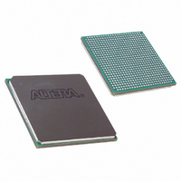
EP2S30F672I4 Altera, EP2S30F672I4 Datasheet - Page 88

EP2S30F672I4
Manufacturer Part Number
EP2S30F672I4
Description
IC STRATIX II FPGA 30K 672-FBGA
Manufacturer
Altera
Series
Stratix® IIr
Datasheet
1.EP2S15F484I4N.pdf
(238 pages)
Specifications of EP2S30F672I4
Number Of Logic Elements/cells
33880
Number Of Labs/clbs
1694
Total Ram Bits
1369728
Number Of I /o
500
Voltage - Supply
1.15 V ~ 1.25 V
Mounting Type
Surface Mount
Operating Temperature
-40°C ~ 100°C
Package / Case
672-FBGA
Family Name
Stratix II
Number Of Logic Blocks/elements
33880
# I/os (max)
500
Frequency (max)
711.24MHz
Process Technology
90nm (CMOS)
Operating Supply Voltage (typ)
1.2V
Logic Cells
33880
Ram Bits
1369728
Operating Supply Voltage (min)
1.15V
Operating Supply Voltage (max)
1.25V
Operating Temp Range
-40C to 100C
Operating Temperature Classification
Industrial
Mounting
Surface Mount
Pin Count
672
Package Type
FC-FBGA
Lead Free Status / RoHS Status
Contains lead / RoHS non-compliant
Number Of Gates
-
Lead Free Status / Rohs Status
Not Compliant
Other names
544-1899
EP2S30F672I4
EP2S30F672I4
Available stocks
Company
Part Number
Manufacturer
Quantity
Price
Company:
Part Number:
EP2S30F672I4
Manufacturer:
ALTERA
Quantity:
3 000
Company:
Part Number:
EP2S30F672I4N
Manufacturer:
ALTERA
Quantity:
238
I/O Structure
Figure 2–54. Stratix II IOE in DDR Output I/O Configuration
Notes to
(1)
(2)
(3)
2–80
Stratix II Device Handbook, Volume 1
Column, Row,
Interconnect
or Local
All input signals to the IOE can be inverted at the IOE.
The tri-state buffer is active low. The DDIO megafunction represents the tri-state buffer as active-high with an
inverter at the OE register data port. Similarly, the aclr and apreset signals are also active-high at the input ports
of the DDIO megafunction.
The optional PCI clamp is only available on column I/O pins.
ioe_clk[7..0]
Figure
2–54:
clkout
aclr/apreset
sclr/spreset
ce_out
oe
Chip-Wide Reset
Output Register
Output Register
OE Register
OE Register
ENA
D
CLRN/PRN
D
CLRN/PRN
D
CLRN/PRN
D
CLRN/PRN
ENA
ENA
ENA
Q
Q
Q
Q
Notes
Used for
DDR, DDR2
SDRAM
clk
Open-Drain Output
(1),
Drive Strength
Pin Delay
(2)
Output
Control
OE Register
t CO Delay
V CCIO
V CCIO
Altera Corporation
PCI Clamp (3)
Termination
On-Chip
Bus-Hold
Circuit
Programmable
Pull-Up
Resistor
May 2007


