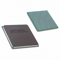
EP2S30F672I4 Altera, EP2S30F672I4 Datasheet - Page 41

EP2S30F672I4
Manufacturer Part Number
EP2S30F672I4
Description
IC STRATIX II FPGA 30K 672-FBGA
Manufacturer
Altera
Series
Stratix® IIr
Datasheet
1.EP2S15F484I4N.pdf
(238 pages)
Specifications of EP2S30F672I4
Number Of Logic Elements/cells
33880
Number Of Labs/clbs
1694
Total Ram Bits
1369728
Number Of I /o
500
Voltage - Supply
1.15 V ~ 1.25 V
Mounting Type
Surface Mount
Operating Temperature
-40°C ~ 100°C
Package / Case
672-FBGA
Family Name
Stratix II
Number Of Logic Blocks/elements
33880
# I/os (max)
500
Frequency (max)
711.24MHz
Process Technology
90nm (CMOS)
Operating Supply Voltage (typ)
1.2V
Logic Cells
33880
Ram Bits
1369728
Operating Supply Voltage (min)
1.15V
Operating Supply Voltage (max)
1.25V
Operating Temp Range
-40C to 100C
Operating Temperature Classification
Industrial
Mounting
Surface Mount
Pin Count
672
Package Type
FC-FBGA
Lead Free Status / RoHS Status
Contains lead / RoHS non-compliant
Number Of Gates
-
Lead Free Status / Rohs Status
Not Compliant
Other names
544-1899
EP2S30F672I4
EP2S30F672I4
Available stocks
Company
Part Number
Manufacturer
Quantity
Price
Company:
Part Number:
EP2S30F672I4
Manufacturer:
ALTERA
Quantity:
3 000
Company:
Part Number:
EP2S30F672I4N
Manufacturer:
ALTERA
Quantity:
238
Figure 2–21. M4K RAM Block Control Signals
Altera Corporation
May 2007
Dedicated
Row LAB
Clocks
Local
Interconnect
Local
Interconnect
Local
Interconnect
Local
Interconnect
Local
Interconnect
Local
Interconnect
Local
Interconnect
Local
Interconnect
The M4K RAM blocks allow for different clocks on their inputs and
outputs. Either of the two clocks feeding the block can clock M4K RAM
block registers (renwe, address, byte enable, datain, and output registers).
Only the output register can be bypassed. The six labclk signals or local
interconnects can drive the control signals for the A and B ports of the
M4K RAM block. ALMs can also control the clock_a, clock_b,
renwe_a, renwe_b, clr_a, clr_b, clocken_a, and clocken_b
signals, as shown in
The R4, C4, and direct link interconnects from adjacent LABs drive the
M4K RAM block local interconnect. The M4K RAM blocks can
communicate with LABs on either the left or right side through these row
resources or with LAB columns on either the right or left with the column
resources. Up to 16 direct link input connections to the M4K RAM Block
are possible from the left adjacent LABs and another 16 possible from the
right adjacent LAB. M4K RAM block outputs can also connect to left and
right LABs through direct link interconnect.
RAM block to logic array interface.
6
clock_a
clock_b
Figure
clocken_a
2–21.
clocken_b
Stratix II Device Handbook, Volume 1
renwe_a
Figure 2–22
renwe_b
Stratix II Architecture
aclr_a
shows the M4K
aclr_b
2–33


